New MEMS metasurface technology allows tunability, adaptability
Electronics and handheld devices such as wearables, smartphones, and tablets continue to get smaller, lighter, and more compact. Optical devices, however, have been slow to follow suit, as the working principle of refractive optical components such as lenses hasn’t deviated much from their inception. A team in Norway is now working to change that with a new tunable lens.
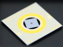
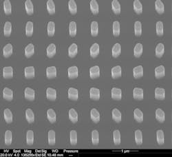
In their study, published in Optics Letters, the team from SINTEF Smart Sensors and Microsystems (Trondheim, Norway) used metasurfaces—ultrathin planar optical components composed of subwavelength nanostructures that manipulate light—to develop a MEMS (micro-electro-mechanical system) tunable dielectric lens.
Metasurfaces are ideal for ultracompact optical devices because they can be subwavelength-thin and with micro- and nanofabrication techniques, according to the researchers, are easily integrated into the manufacture of smaller devices.
The new MEMS-tunable dielectric metasurface lens works similar to the lens within the eye, bringing objects at different distances into focus. “While the lens within your eye achieves this through deformation by muscular straining or relaxing, our device does this by shifting the distance between two metasurface lenses,” says Christopher Dirdal, a research scientist at SINTEF Smart Sensors and Microsystems. Thin-film piezoMEMS (piezoelectric MEMS) architecture made this shift possible.
“Tunable metasurfaces offer a range of new possibilities and piezoMEMS is an excellent platform to harness those,” he says.
The focal length changes when applying low voltage—a quarter of that used in existing similar technology. The researchers did this to lead zirconate titanate (PZT) membranes (which are around 25 times thinner than a strand of hair), causing them to deform. Tunability in traditional optical systems requires bulky, power-consuming components (i.e., stepper motors, rotators, or magnets).
To get to this point, the researchers fabricated a metasurface chip and inserted it into a MEMS actuator designed for piston and tip/tilt movements (see figures). They used nanoimprinting, in which a mask of nanostructures is pressed and the resulting pattern transfers to a silicon substrate via deep-reactive ion etching, explains Dirdal. “The metasurface structure is designed to act as a lens,” he says.The team measured the focus shift through the distance the objective lens needed to be moved to regain focus upon full-range MEMS displacement of the metalens. By applying 23 V, they achieved an approximately 250 μm focal length shift by placing the metasurface 7.2 μm away.
MEMS metasurfaces can also act as a varifocal lens doublet. To demonstrate this, a second metasurface lens was placed after the MEMS metasurface. The two were held in place by separate holders that can be moved relative to each other for ease of alignment. And the separation distance between the lenses is varied by the MEMS displacement, which allowed the team to tune and adapt the focal point of the lens doublet.
“Most systems incorporating metasurfaces so far are static, meaning the optical functionality is locked after fabrication,” Dirdal says. But tunability and adaptability are necessary for applications such as cameras, 3D-mapping lidar systems, drone-based mapping, and holographic displays.
The MEMS metasurface technology also shows potential for biomedical applications—portable diagnostic instruments, for example—because it allows imaging of tissue at different depths to better see and study things like neurons and blood vessels.
Dirdal says his team is now looking to further optimize its MEMS architecture to develop a commercially relevant tunable lens device. “We’re interested in further exploring the combination of MEMS and metasurfaces for various applications where there is a need for small, light, cheap optics without compromises to optical quality,” he adds.
About the Author
Justine Murphy
Multimedia Director, Digital Infrastructure
Justine Murphy is the multimedia director for Endeavor Business Media's Digital Infrastructure Group. She is a multiple award-winning writer and editor with more 20 years of experience in newspaper publishing as well as public relations, marketing, and communications. For nearly 10 years, she has covered all facets of the optics and photonics industry as an editor, writer, web news anchor, and podcast host for an internationally reaching magazine publishing company. Her work has earned accolades from the New England Press Association as well as the SIIA/Jesse H. Neal Awards. She received a B.A. from the Massachusetts College of Liberal Arts.


