Source-mask optimization using thick masks improves EUV lithography
While most photolithographic systems that are used to fabricate silicon computer chips operate at the 193 nm deep-ultraviolet (DUV) wavelength, extreme-ultraviolet (EUV) lithographic systems are now being used in growing quantities to fabricate leading-edge chips with achievable feature sizes on the order of 5 nm, and will become more widely used in the future. Due to the 13 nm wavelength, the high required resolution, and the large field size needed, EUV systems are some of the most precise optical systems known. This required precision extends to the photomasks whose patterns are imaged onto the wafers for exposure.
As the smallest feature size (otherwise known as the critical dimension, or CD) on the mask is made smaller, optical-proximity effects (OPEs), in which the linewidth of an isolated line fabricated on the wafer is different from the linewidth of dense lines fabricated on the wafer (even though the linewidths are the same on the mask), becomes more of a problem. Many tricks have been conceived and used to correct for OPE, but these tricks become harder to use at very small CDs. One approach used is computational lithography, which refers to techniques that improve the resolution and process window by optimizing the illumination source and mask pattern with mathematical models and optimization algorithms, without changing the hardware and software configurations of the lithography systems. The mask pattern, for example, ends up having modifications to feature shapes to counteract the proximity effect.
Researchers from the Shanghai Institute of Optics and Fine Mechanics (SIOM) of the Chinese Academy of Sciences (CAS; Beijing, China) have created a computer model from which has arisen a proposed source-mask optimization (SMO) technique for EUV lithography based on a thick mask; the model is driven by a social learning particle swarm optimization (SL-PSO) algorithm.1 SMO is a critical computational lithography technique in which the illumination source and mask pattern are simultaneously optimized to improve imaging quality. The researchers’ simulation results indicate that the technique is superior to similar SMO techniques based on heuristic algorithms in optimization efficiency.
Multiswarm learning
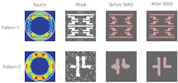
Particle learning optimization, which has been around for many years, has been augmented by the more-recent addition of “multiswarm learning,” in which so-called learning objects modeled in the software are subjected to somewhat-randomized interactions, but with parameters that select the best learning objects; the algorithm eventually converges on a solution. The researchers’ fast thick-mask model, based on a structure decomposition method (SDM), was used to simulate images of the pixelated mask; the simulation accuracy was improved compared with the previous thin-mask model (see figure). Rigorous electromagnetic simulation was then carried out to validate the optimization results. The source (basically, the illumination pattern at the pupil plane of the optics) and the mask pattern were optimized together using the SL-PSO algorithm.
An initialization parameter was tuned to control the initial swarm in the SL-PSO algorithm; the optimization efficiency and the optimized mask’s manufacturability were both improved, as evidenced by the reduction of pattern errors between the print image and the target pattern for three patterns of 94.7%, 76.9%, and 80.6%, respectively.
The researchers say they now must increase the number of mask pixels that their algorithm can effectively handle.
REFERENCE
1. Z. Zhang et al., Opt. Express (2021); https://doi.org/10.1364/oe.418242.

John Wallace | Senior Technical Editor (1998-2022)
John Wallace was with Laser Focus World for nearly 25 years, retiring in late June 2022. He obtained a bachelor's degree in mechanical engineering and physics at Rutgers University and a master's in optical engineering at the University of Rochester. Before becoming an editor, John worked as an engineer at RCA, Exxon, Eastman Kodak, and GCA Corporation.
