NANOPOSITIONING: Piezoelectric nanopositioners forge low-cost atomic force microscope
JAMES F. MacKAY, BEAU BROSSMAN, and SHANNON GHORBANI
Scanning probe microscopy (SPM) was invented 30 years ago, and commercial SPM instruments have been available for nearly that long. Today there are many types of SPM systems, including atomic force microscopes (AFMs), but they all work in a similar manner: A scanner moves a surface-sensitive probe in a raster motion (x, y) over the surface of a sample, while the output signal of the probe is used to control the vertical height (z) of the probe above the surface. The response of the probe to the surface is then used to create a topographical image of the surface in x, y, and z. Motion control for SPM instruments is typically provided by a piezoelectric actuator of some form.
Although SPM systems are generally viewed as expensive imaging tools for academic research and high-end commercial applications such as semiconductor manufacturing, a large number of applications such as industrial wear testing, surface-property studies, and optical antenna studies could benefit from the high-resolution imaging capabilities of SPM; however, they are prohibited by the expense and skill level required by most available instruments.
For years, companies that sell SPM systems have offered nanopositioners as “upgrade” features. The motivation is clear, given that nanopositioners offer integrated absolute metrology position sensors, closed-loop feedback control, sub-nanometer resolution, and exceptional scan linearity. Commercial nanopositioners are extremely robust and offer linear motion without the creep, hysteresis, or arching motion that is associated with bare piezoactuators. Some SPM companies have also integrated nanopositioners into their standard products for improved performance. This type of integration tends to increase the price of the SPM as a result of the improved performance over bare piezoactuators or tube scanners.
Because prices for nanopositioners continue to fall despite ongoing improvements in resolution, linearity, and reliability, an alternative to purchasing a commercial SPM instrument is to build a high-quality, cost-effective system from off-the-shelf nanopositioners and standard optical components. As a nanopositioning company, Mad City Labs has sold many stages as retrofit scanners for existing SPM systems, and we frequently sell the components to customers that wish to build their own system.
Surface-probe considerations
When building your own SPM instrument, there are several decisions to make early on in the process. The type of surface-sensitive probe will determine which type of nanopositioner is required for the application. Many commercial SPM systems use an optical deflection method to measure the surface/probe interaction. While this technique is very effective and yields high-resolution images, it requires probe alignment and significant skill by the operator. Furthermore, it takes significant knowledge and skill to build such a probe system.
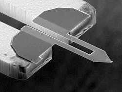
The Nanosensors (Neuchâtel, Switzerland) Akiyama-probe (www.akiyamaprobe.com) or A-probe, a resonant sensor, has recently become commercially available (see Fig. 1). Like all tuning-fork-based sensors, the Akiyama-probe is “self sensing” and does not require any alignment. Tuning-fork sensors are easy to install and operate using specialized electronics. In the Akiyama-probe, the probe tip/cantilever is attached between the tines of a standard tuning fork. As the tuning fork vibrates, the cantilever oscillates up and down. When the tip interacts with the surface under test, the vibration frequency of the tuning fork changes and can be used as a control signal to move the z-axis nanopositioner up or down to maintain constant vibration frequency.
The oscillation amplitude of the Akiyama-probe is about 1 µm, which is quite large, resulting in a probe that is very robust but with less surface sensitivity than an optical deflection probe. Because of the large oscillation amplitude, the Akiyama-probe is not easily damaged by a coarse surface approach.
As a second example, a standard tuning fork can be used as a resonant probe by attaching an etched tungsten wire to one of the tines. This type of homemade probe is less robust and more easily damaged than the Akiyama-probe, but it has much smaller oscillation amplitude and better surface sensitivity.
Both types of resonant probes require phaselocked-loop detection techniques to convert a tip/surface interaction frequency change to a voltage that is usable as a control signal. The Mad City Labs MadPLL instrumentation package performs this function while providing complete signal conditioning for resonant sensors. It comes with a probe board and probe sensor preamplifier and has automated parasitic capacitance compensation, an integrated z-axis proportional integral loop controller, and a USB 2.0 interface for total software control. When using the Akiyama-probe, the sensor can be changed in a few seconds since electronic setup of a new sensor probe is fast and completely automated. The ease of tip exchange and software automation reduces the expertise necessary to use this type of instrument.
Selecting a nanopositioner
When selecting a nanopositioning system for an SPM instrument, the z-axis is the most critical. For many applications, we recommend that the z-axis be decoupled from the x, y raster scanner. Although there are several very good three-axis nanopositioners for SPM applications, most integrated systems have a relatively slow z-axis.
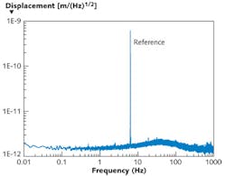
For most resonant probe applications, a z-axis resonant frequency of 2 kHz is sufficient. We recommend a direct-drive single-axis stage that has been designed for true flexure-guided motion: The z-axis should have an integrated Mad City Labs PicoQ position sensor or equivalent and ideally have a range of motion of about 30 µm. The integrated PicoQ sensor is suited for SPM applications because it offers very low noise, very low drift, high frequency response, and high linearity without creep or hysteresis (see Fig. 2). For a stage driven with a 0.6 nm peak-to-peak sine wave reference at 6.5 Hz, the stage has position noise at frequencies below 1 Hz, which means that the z-axis will have low drift while scanning.In addition, there is no need for additional calibration of the z-axis motion when the integrated sensor is used to track the topography of a surface. When used with a resonant sensor and the MadPLL package, the z-axis stage must be switched into open-loop mode so that the position of the z-axis may be controlled to keep the vibration frequency of the resonant probe constant.
The next nanopositioner selection is the x, y raster scanner. While the z-axis range of motion is kept to 30 µm for reduced noise, the same consideration is not as important for x, y scanning; however, out-of-plane motion is an important consideration. Always select a scanner that uses true flexure-guided motion, as this will provide the smoothest, most repeatable scan without out-of-plane motion. For most SPM applications, a 50–100 µm range of x, y motion is sufficient; on the other hand, scanners with up to 200 µm motion ranges are commonly available.
A further consideration when deciding on x, y range of motion is resolution of the digital-to-analog converters (DACs) and analog-to-digital converters (ADCs) that control stage motion. For a 100 µm stage, a 16 bit DAC yields a smallest step size of about 1.6 nm, while a 20 bit DAC has a smallest step size of 0.1 nm. If you wish to perform x, y scans with sub-nanometer step size, then we recommend a 20 bit DAC. For some industrial applications, a 16 bit DAC may be sufficient.
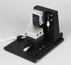
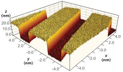
Once nanopositioners have been selected, the next issue is coarse positioning for x, y, and z. Micropositioning stages for coarse positioning—either manual or motorized—can be purchased from one of many optical component vendors. In fact, the optical breadboards and mounting brackets offered for standard optics construction are ideal for the base and tower of the homemade SPM system. An option to consider is a motorized coarse z-stage to allow for a higher level of automation and aid in sample approach when using delicate probes. A video microscope can be added using lens tubes, a microscope objective, and a low-cost video camera.The entire SPM setup should be installed on a vibration-isolation table and covered with an enclosure to reduce microphonics and air currents that can cause drift; again, these components are available as standard optical hardware and Mad City Labs can even provide a bill of materials for sample SPM systems we have constructed (see Fig. 3; also see www.madcitylabs.com/afmvideo.html). These self-built SPM systems can easily image 20-nm-high steps in silicon with sub-nanometer resolution capability (see Fig. 4). With the ready availability of high-quality nanopositioners and resonant sensors, SPM instruments for imaging materials and studying optical antennas are now easier to build than ever before.
ACKNOWLEDGMENT
MadPLL and PicoQ are registered trademarks of Mad City Labs.
James F. MacKay is a member of the R&D Group and Beau Brossman is an applications engineer at Mad City Labs, 2524 Todd Drive, Madison, WI 53713; e-mail: [email protected]; www.madcitylabs.com. Shannon Ghorbani is a product development manager at Mad City Labs GmbH, Balz-Zimmermann-Str. 7, CH-8302 Kloten, Switzerland.


