CMOS detectors: TCAD simulation of image sensors catches light in silicon
Technology CAD simulation is helping designers of CMOS image sensors meet the challenges presented by increasing device complexity and decreasing pixel size.
BIJU JACOB, ALP GENCER, GERGO LETAY, AND PAUL PFAEFFLI
Fueled by increasing market demands, CMOS image-sensor technology has been pushed to its limits by advances in semiconductor technology and pixel architecture.1 Manufacturers have recently developed image sensors with pixel pitch below 2.5 µm. And on the pixel architecture front, design has moved from traditional active pixel sensor (APS) to shared pixel and pinned photodiode APS.
Pixel dimensions shrink as a consequence of technology scaling, so it also becomes increasingly difficult for the pixel to collect light efficiently and convert it into useful electrical signals. Novel pixel architectures also pose technological challenges to the design of the photodiode and active electronic components within the pixel. Technology computer-aided design (TCAD) can accelerate the realization of compact and novel pixels while also reducing time-to-market.2
Pixel back-end
Technology CAD simulation of CMOS image sensors consists of three parts: process simulation, in which structure and doping profiles are simulated according to the CMOS process flow; optical simulation, consisting of light collection into the pixel, color-filtering, and optical absorption in silicon to generate electron-hole pairs; and electrical simulation, consisting of charge transfer and other signal-processing tasks specific to the pixel architecture.
The optical simulator accepts a spectral irradiance image on the image sensor surface as input and provides the electrical simulator with the optical-generation rates (of conversion of photons to electron-hole pairs). For operation within the visible optical range of the electromagnetic spectrum, the pixel dimensions are on the order of a few wavelengths of the incident light. Diffraction and interference effects dominate the optical propagation of light through these compact pixels. An accurate and computationally efficient simulation approach is required to model and optimize the optical efficiency of the image sensor.3
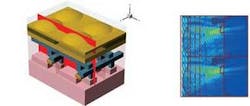
A simple image-sensor pixel consists of a spherical microlens (in reality, more complicated microlens geometry is used), various back-end layers (such as color filter, planarization, and passivation), metal interconnects, photodiode, and one transistor. The absolute electric field is computed with Sentaurus Device EMW (a full-wave Maxwell solver based on the finite-difference-time-domain (FDTD) method) in a 2-D cross section of a two-pixel system for an incident monochromatic plane wave with a wavelength of 400 nm. The lateral and vertical dimensions of the pixel are 2.4 and 6 µm, respectively (see Fig. 1). Upon comparing the optical field patterns of the structure with and without the microlens, it becomes apparent that the microlens focuses light onto the photodiode, thereby increasing the amount of captured light.
In addition to enhancing pixel sensitivity, it is also crucial in the image-sensor back-end design to suppress unwanted light from neighboring pixels (optical crosstalk). So modeling of light propagation and carrier generation becomes necessary, using TCAD tools that incorporate realistic geometry, material properties, and excitation conditions (see Fig. 2).
null
The photodiode
The photodiode in the image sensor in our example consists of an n-type material sandwiched inside a p-type region. It turns incident light into electron-hole pairs (at a characteristic optical-generation rate) and stores them until they are transferred to the readout node when the gate is turned on. To perform this task, the n-type well of the photodiode must be carefully engineered. If the doping level inside the well is too high, then the electrons do not flow out of it. If it is too low, not enough electrons are collected. Moreover, the distance from the well to the channel region of the transfer gate also plays a critical role.
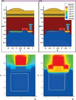
Technology CAD simulation provides an efficient and cost-effective approach to balance this tradeoff. While process simulation helps the designer optimize the structure and the doping profile of the pixel, subsequent device simulation helps to determine the efficiency of the photodiode cycling between the “filled” and “emptied” state. Counting the number of electrons in each state determines the drain efficiency (defined as 1 - Nfill/Nempty).
In this sensor, the transfer transistor is narrower than the photodiode. Although a narrow gate results in a more compact design, it also decreases the collection efficiency of electrons. Using 3-D process and device simulation of the entire cell, this tradeoff can also be evaluated (see Fig. 3).
null
TCAD-driven optimization
Once a TCAD simulation flow has been established and calibrated, it enables accurate analysis of the influence of process parameters on device characteristics, and consequently addressing and controlling of process variability as needed in the manufacturing process. In other words, complete process design flow and comprehensive device modeling allow quantification of a process-device relationship.
The challenge is to extract the relevant data from the wealth of information produced by simulation to give statistically meaningful results. As a first step, a multidimensional response surface model is fitted to the data, providing correlation information for process variations, design parameters, and observation parameters-collectively called a process compact model. While TCAD simulations typically take hours, the PCM can be evaluated immediately.
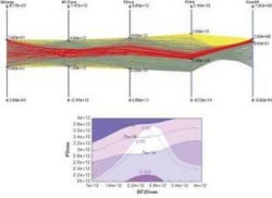
In the sensor model from the previous section, one important design optimization task is to maximize the drain efficiency (DrainEff) and the number of initially collected electrons of the photodiode (PDfull). This can be achieved by optimizing implant conditions such as the implant energy of boron (BEnergy), boron dosage (BF2Dose), and phosphorus dosage (PDose). Due to the low number of input variables, a full factorial design of experiments (DOE) with 72 experiments can be chosen. To make more-complex variations feasible and greatly reduce the number of necessary experiments, it is essential to exploit all negligible interaction terms and use fractional factorial DOEs.
The process compact model is usually visualized using a matrix of scatter pair plots. The scatter plots reveal relationships between two variables, which manifest themselves by any nonrandom structure in the plot. For better visualization, the parallel coordinate plot was devised to represent multidimensional information.4 By drawing the axes parallel to each other, arbitrary dimensional data can be represented in a 2-D plot, restricted only by the width of the page it is printed on. Each variable of a data point is plotted on its own axis, and straight lines connect variable values on adjacent axes. Therefore, a point in a multidimensional space becomes a polygonal line (see Fig. 4). Obviously, the target can only be met for a limited range of boron and phosphorus dosage within which the boron energy can be varied over the entire investigated range. By changing the constraint limits, the system behavior can be studied interactively.
null
REFERENCES
1. K.H. Paik et al., Conf. Proc. SISPAD 2005, Tokyo.
2. A. El Gamal et al., IEEE Circuits & Devices Magazine 21 (2005).
3. P.B. Catrysse et al., J. Opt. Soc. Am. A, 19(8), 1610 (2002)
4. A. Inselberg et al., Human-Machine Interaction Systems 1, 199 (1991).
BIJU JACOB is senior corporate applications engineer, ALP GENCER is senior corporate applications engineer for TCAD products, GEORGE LETAY is senior corporate applications engineer and product manager for optoelectronics, and PAUL PFAELLI is manager of TCAD support Europe at Synopsys Switzerland, Affolternstrasse 52, CH-8050, Zurich, Switzerland; e-mail: [email protected]; www.synopsys.com.


