TECHNOLOGY REVIEW 2011: Photonics reaches from science to the consumer world
One of the characteristics of good technology is that it becomes more accessible over time. Once-esoteric technology is integrated into the home, workplace, and automobile (laser computer mice, LED headlights, and computer-game motion sensors); in other cases, very exotic technology is transformed into something that could be called pragmatically exotic (such as quantum cryptography).
Because we at Laser Focus World are happy to contribute our own slant on this year’s hoopla in the general press over transformative technology (the iPad, smart phones, and such seem to lead the way), we’ll start off the 2011 Technology Review by covering photonics innovations that in some way appeal to the general public.
Technology for everyone
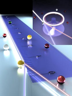
The push to develop white-light LEDs that are efficient and low enough in cost for general illumination has resulted in drastic increases in LED efficiency (usually stated as luminous efficacy, in lm/W) over more than a decade of research. However, LEDs suffer from efficiency droop, in which their highest efficiencies (up to 265 lm/W) are demonstrated at very low light levels; as the drive current is turned up to produce a useful amount of light, the efficiency drops to levels that are less remarkable. Researchers at the University of New Mexico, Sandia National Laboratories (both of Albuquerque, NM), and the National Institute for Standards and Technology (NIST; Gaithersburg, MD) have created a four-color source consisting of lasers—which don’t suffer efficiency droop—to test whether laser light has high-enough color-rendering quality for illumination (see Laser Focus World, August 2011, pp. 17–18). A red laser diode is combined with yellow, green, and blue solid-state lasers in the test device. The result: Yes, the source was at least as pleasing to the eye as white-light LEDs. A future all-laser-diode-based source could be far more efficient than any type of LED.
In a somewhat similar vein, BMW (Munich, Germany) is experimenting with using blue laser diodes combined with a yellow phosphor to form white-emitting laser headlights. The advantages include beams that spread less, higher efficiencies, and, because the lasers are smaller than LEDs, opportunities for novel styling.
Digitally capturing the motions of a person for use in computer-generated movies or games is usually done in a single, staged setting (the most well-known example is Microsoft’s Kinect motion sensor, which uses an array of infrared [IR] beams and sensors to determine the motions of gamers cavorting in front of the device). But the ability to capture motion outdoors without a stage would allow people to stage scenes anywhere, anytime, moving wherever they want. A collaboration between Disney Research and Carnegie Mellon University (both in Pittsburgh, PA) has achieved just this. A wearable harness contains 16 or more small video cameras pointing every which way; after an initial calibration with respect to a reference structure, the position of each camera is known with respect to the person wearing the harness. In use, the wearer can walk, run, and gesture; each camera captures a different view, with all views knit together by software to track the motion of the wearer’s limbs and torso (see Fig. 1). With technology like this, all the world is a stage (or a game).
While commercial electronic readers such as the Amazon Kindle rely on the E-Ink (Cambridge, MA) electrophoretic technology to provide an easy-to-read black-and-white display, other technologies are being developed that have the potential for higher contrast. One example is electrowetting, in which each pixel holds a pigmented fluid (often black) that is moved around via an applied voltage to expose or hide a background (usually white). Such displays have been hampered by the high voltages needed to move the droplets. A group at the Massachusetts Institute of Technology Lincoln Laboratory (Lexington, MA) and Tufts University (Medford, MA) has developed an improved electrowetting system using lipid bilayers on hafnium oxide films as a reversibly wettable dielectric that change the droplet’s wetting angle drastically (between 10° and 140°) with only a small voltage (see Laser Focus World, September 2011, pp. 10–11). The pixels can cycle for days at a time without any degradation.
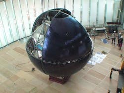
As for high-resolution displays, they all seem to share one characteristic—they’re flat. But this year, Mitsubishi Electronics (Tokyo, Japan) unveiled a large organic-LED (OLED) display that is about as non-flat as possible. Made from an aluminum ball covered with 10,362 OLED panels each 96 × 96 mm in size, the sphere is now hanging in Tokyo’s National Museum of Emerging Science and Innovation (see Fig. 2). With approximately 10 million pixels, the display certainly qualifies as high resolution. The globe is mostly used to display scenes of clouds and other scenes of Earth taken from a meteorological satellite.Leading-edge research
To a nontechnical person, much of what goes on in the world of photonics would be less understandable than these examples, and thus less tangible. But just because a research group isn’t trying to start a consumer craze doesn’t mean its research won’t lead to great benefits. Even the most esoteric research has potential practical uses.
For example, researchers at Cornell University (Ithaca, NY) have created a photonic time cloak, which can create a “time hole” in a beam of light and then remove the hole, allowing an event to happen in the time hole without an observer knowing it (see Laser Focus World, September 2011, pp. 16–18). It does this by speeding up and slowing down the front and rear parts of the beam, respectively, then reversing the process. Based on four-wave mixing, the one-dimensional optical-fiber-based effect was used to hide the beam from a separate pulse, eliminating the nonlinear interaction that would have occurred without the time lens. The device could someday serve as a type of gatekeeper in photonic circuits. The researchers say the device is a step toward a full time-and-space invisibility cloak.
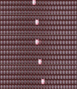
By exhibiting a change in resonance, microrings (both active and passive) and other microcavity resonators can serve as very sensitive particle detectors. Researchers at Washington University (St. Louis, MO) have developed a microring laser that not only detects the presence of nanoparticles—it counts them too, up to as many as 816 (see Fig. 3). Via mode-splitting or resonance shifts, it can detect and count 30-nm-diameter polystyrene particles, 20-nm-diameter gold particles, and influenza A viruses in air, and 60-nm-diameter polystyrene particles in water.A random-number generator created by scientists at the University of Maryland (College Park, MD) and Beijing Normal University (Beijing, China) relies on a superluminescent LED (SLED) to provide two spectrally separated parallel, independent 10 Gbit/s random bit streams (see Laser Focus World, May 2011, pp. 18–20). The device has many potential uses ranging from secure-key generation to gaming.
A group at Vrije Universiteit (Amsterdam, the Netherlands) and Leiden University (Leiden, the Netherlands), which has been using “align-and-shine” photolithography to create patterns such as slits on the ends of optical fibers (see Laser Focus World, May 2009, pp. 21–24), is now using the technique to create low-mass gold cantilevers on the ends of fibers.1 The cantilevers reflect light exiting the fiber back into the fiber (allowing optical interrogation) and can serve as sensitive detectors of biochemical substances for early cancer diagnosis and other applications. The finished cantilevers are 350 nm thick, 22 μm long, and 7 μm wide and have a 447 kHz resonant frequency.
Often, early-stage research consists of design followed by detailed computer modeling, with a successful outcome leading to future fabrication of the device. In just one example, Hamza Kurt of the TOBB University of Economics and Technology (Ankara, Turkey) has confirmed through numerical techniques that, by cascading small photonic-crystal (PC) sections at the end of a PC waveguide, a compact structure is formed that creates a simple and efficient Y-type power divider potentially useful in photonic circuits, wavelength multiplexers, and semiconductor lasers.2 The approach exploits bandgap and self-collimation properties of PCs and was modeled using the finite-difference time-domain method.
Light sources galore
This year, researchers at the Optoelectronics Research Centre, University of Southampton (Southampton, England) have improved on the frequency-doubled fiber laser by creating a version with an enhancement resonator within the fiber-laser’s cavity, allowing operation without active cavity-length stabilization.3 An active ytterbium-doped polarization-maintaining fiber is bounded on one end by a bulk-optic spectrum-narrowing diffraction grating; on the other end is a bulk-optic single-harmonic-generation resonator with a lithium triborate (LBO) nonlinear crystal. The enhancement cavity containing the LBO crystal transmits only resonant axial modes back into the fiber; as a result, the fiber lases only on those axial modes that are phase-matched for frequency-doubling and are resonant in the cavity, leading to high intracavity power. For 90 W of absorbed diode-pump power at 975 nm, the laser emits 15 W of 540 nm light (with more efficient optics, it would emit 19 W).
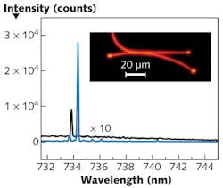
An X-shaped cadmium selenide (CdSe) nanowire cavity devised by a group at Zhejiang University (Hangzhou, China) produces a single-longitudinal-mode output at 734.3 nm with a linewidth of 0.11 nm (see Fig. 5).4 Two 420-nm-diameter CdSe wires are positioned on a magnesium fluoride substrate by tapered fiber probes until they touch over a 6 µm length. The wires are pumped with 15 ns, 532-nm-wavelength laser pulses at a 5 kHz repetition rate.A quantum-dot (QD) laser developed by Japanese scientists at QD Laser and Fujitsu Laboratories Ltd. (both in Kanagawa) and the Institute for Nano Quantum Information Electronics, the University of Tokyo emits light at 1.3 µm even when heated to temperatures up to 220°C. To achieve this, they sidestepped the problem of increased inhomogeneous broadening with QD density by suppressing indium out-diffusion from the self-assembled indium arsenide QDs. The threshold current of the eight stacked QD layers was 15 mA at 30°C and 55 mA at 200°C, and 2 mW output at 210°C. One possible use is optical sensing in deep-oil exploration.
A broadband continuous-wave (CW) optical parametric oscillator that is incoherently pumped has been demonstrated by researchers at the University of Twente (Enschede, the Netherlands), the 2FOM Institute for Plasma Physics Rijnhuizen (Nieuwegein, the Netherlands), and the 3HH Wills Physics Laboratory at the School of Physics (Bristol, England).5 Broadened by noncollinear phase-matching, the OPO has a 230 nm idler spectral bandwidth centered around 3400 nm and an idler output up to 1.4 W. It is pumped with an amplified spontaneous-emission source and is based on a 50-mm-long periodically poled magnesium oxide doped lithium niobate crystal. Uses include spectroscopy and speckle-free imaging.
Innovative photonic devices
Engineers at Toyota (Nagakute, Japan) and the National Institute for Materials Science (Tsukuba, Japan) are developing plasmon-based color filters for use in automotive applications, spurred by the greater durability of metal-based filters over dye filters.6 Optically thick aluminum films on quartz have hexagonal or square arrays of subwavelength holes, with some devices having circular holes (polarization-independent output) and others triangular holes (polarization-dependent output) or other shapes. The transmitted color varies depending on the lattice spacing, while the bandwidth depends on the hole shape. Colors were obtained throughout the visible with bandwidths on the order of 100 nm.
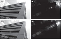
Meanwhile, at Nikon (Kanagawa, Japan), development engineers are interested in creating higher-performance optical coatings for digital cameras, which (unlike film cameras) suffer diffraction from the image sensor and reflections from the required low-pass filter. Because antireflection (AR) coatings benefit from films that have a very low refractive index, the engineers have introduced an ultralow-index layer into AR coatings made of porous fluoride layers fabricated with the sol-gel process (example index: 1.26).7 The technique avoids the problems associated with previous sol-gel metal oxide coatings such as water absorbance and low transmittance in certain regions. The filters perform beautifully for visible wavelengths and IR wavelengths as well (see Fig. 6).A 3D negative-index metamaterial (see Laser Focus World, August 2011, pp. 15–16) created by researchers at the University of Illinois at Urbana-Champaign, the US Navy NAVAIR-Naval Air Warfare Center Weapons Division (China Lake, CA), and Sandia National Laboratories (Albuquerque, NM) is created through nanoimprint lithography; the resulting silicon stamp, coated with multiple layers, is used to “print” the metamaterial onto any desired substrate—which can be rigid or flexible. The process satisfies a previously unmet need: a way to fabricate large amounts of high-quality 3D metamaterial quickly out of a durable, useful material. The result has a strongly negative refractive index, useful for superlenses, invisibility cloaks, novel resonators, and other photonic components.
A luminescent solar film developed at Shanghai Normal University (Shanghai, China) is meant to be coated on crystalline silicon photovoltaic (PV) solar cells. The coating serves two purposes: It acts as an AR coating, while also absorbing some UV light and downconverting it to near-IR photons that are more efficiently absorbed by the PV cell.8 The bilayer nanoporous film contains a downconverting ytterbium-doped vanadate layer and a silicon dioxide (SiO2) layer to reduce reflection. The film raised transmission by 3.7% from 500 to 800 nm, while providing photoemission in the range of 950 to 1100 nm.
A broadband organic photodetector created by scientists at Chinese Academy of Sciences (Changchun, China) and the City University of Hong Kong has a broad spectral-response range spanning 200 to 900 nm.9 Based on small-molecule materials, the detector has a 20% external quantum efficiency over its entire range. The use of two different donor-acceptor heterojunctions allowed photoresponses over the deep-UV and visible-to-near-IR regions were independently optimized. The fast response time of 56 ns could enable military applications as well as sensing and communications.
Graphene makes its mark
Science writers rave about graphene—not because it’s the only new thing to write about but because it has unique properties: the highest tensile strength known, relatively high conductivity, and, with doping or other modifications, interesting semiconductor properties. Researchers at the University of Manchester (Manchester, England) and Free University Berlin (Berlin, Germany) have taken advantage of the impermeability of graphene to gases to create small graphene bubbles on a SiO2 substrate; the bubbles, which act as microlenses with fluid either underneath or on top, can be manipulated by applied voltages that change the lenses’ focal length.10 Lenses from 5 to 20 µm in diameter were fabricated. In a typical example, the radius of curvature of one bubble changed from 31.3 µm at 0 V to 26.7 µm at -35 V.
Three scientists at the University of Tokyo are using graphene to passively modelock fiber lasers.11 The absorption of graphene is relatively wavelength-independent and is saturable, with fast response time and a large modulation depth. Mechanically exfoliated (in other words, separated from graphite using Scotch tape) multilayer graphene films were placed on the end of an optical fiber that was butt-coupled to another fiber and inserted into an erbium-doped fiber-laser ring cavity. The 1566-nm-emitting laser produced a modelocked pulse train of 6.22 MHz.
A graphene-based quantum Hall-effect IR photodetector created by researchers at New Mexico Tech (Socorro, NM), the University of California–Riverside, and the Center for Integrated Nanotechnologies and Sandia National Laboratories (Albuquerque, NM) functions at 70 K, a temperature reachable using liquid nitrogen in the vapor-evacuation regime (a relatively easy way to cryogenically cool detectors).12 The responsivity at 10.6 µm was in the range of 10-2 to 10-3 V/W, with a 0.5 µV noise that could be dramatically reduced with a different geometry.
Optical fibers for many purposes
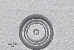
A group at the University of Maryland and the NIST Center for Nanoscale Science and Technology has demonstrated superfocusing of light using an optical-fiber-based surface plasmonic lens.13 Fabricated directly on the end of an optical fiber using focused ion-beam milling, the lenses have up to four concentric annular slits and focus at distances of only a few microns away from the lens (see Fig. 7). Because the slit widths are smaller than the wavelength, light passes through the slits only as surface-plasmon polariton (SPP) modes that are coupled back to optical waves at the exit of the slits. Moreover, the SPP propagation delay can be controlled by the width of the slits to induce a curved wavefront and a tight focus at the desired distance. The lens achieves a spot size of 450 nm ±60 nm, which is below the diffraction limit for the 808 nm light.A single 5.4-km-long holey fiber with an ultrabroadband photonic-transport system developed by researchers at the National Institute of Information and Communications Technology (Tokyo, Japan) and Aoyama Gakuin University (Kanagawa, Japan) transmits simultaneous 3 × 10 Gbit/s optical data streams in the 1059 nm, C- (1550 nm), and L- (1569 nm) wavebands.14 The fiber is singlemode for all wavelengths and has transmission losses at the three wavelengths of 1.42, 1.07, and 1.08 dB/km, respectively. Clear eye-diagram openings were observed and error-free transmissions were achieved.
A widefield optical receiver for free-space optical communications created by engineers at Johns Hopkins University (Laurel, MD) is based on a fiber-optic-bundle array.15 Each fiber in the bundle is paired with a lens in a microlens array; a position-sensitive detector controls mechanics that position the lens array such that a communications beam incident at an arbitrary angle is always coupled into all the fibers. The fiber bundle then routes the light to remotely located detectors. The 1-mm-diameter lenses match the 0.37 numerical-aperture, 200-µm-core fibers; the motion stage has a 100 µm range. The prototype was operated at ±10°; simulations showed effectiveness at larger angles.
REFERENCES
1. K. Babaei Gavan et al., Opt. Lett., 36, 15, 2898 (Aug. 1, 2011).
2. H. Kurt, Appl. Opt., 50, 27, 5256 (Sept. 14, 2011).
3. R. Cieslak and W.A. Clarkson, Opt. Lett., 36, 10, 1896 (May 15, 2011).
4. Y. Xiao et al., Appl. Phys. Lett., 99, 023109 (2011).
5. J. Storteboom et al., Opt. Exp., 19, 22, 21786 (Oct. 24, 2011).
6. D. Inoue et al., Appl. Phys. Lett., 98, 093113 (2011).
7. T. Murata et al., Appl. Opt., 50, 9, C403 (Mar. 20, 2011).
8. Y. Peng et al., Appl. Phys. Lett., 99, 121110 (2011).
9. S. Wu et al., Appl. Phys. Lett., 99, 023305 (2011).
10. T. Georgiou et al., Appl. Phys. Lett., 99, 093103 (2011).
11. A. Martinez et al., Appl. Phys. Lett., 99, 121107 (2011).
12. N.G. Kalugin et al., Appl. Phys. Lett., 99, 013504 (2011).
13. Y. Liu et al., Opt. Exp., 19, 21, 20233 (Oct. 10, 2011).
14. N. Yamamoto et al., Opt. Exp., 18, 5, 4695 (Mar. 1, 2011).
15. D.V. Hahn et al., Opt. Lett., 35, 21, 3559 (Nov. 1, 2011).

John Wallace | Senior Technical Editor (1998-2022)
John Wallace was with Laser Focus World for nearly 25 years, retiring in late June 2022. He obtained a bachelor's degree in mechanical engineering and physics at Rutgers University and a master's in optical engineering at the University of Rochester. Before becoming an editor, John worked as an engineer at RCA, Exxon, Eastman Kodak, and GCA Corporation.


