Technology Review: Laser Focus World’s top 20 photonics technology picks for 2018
Perhaps you believe that the rate of technical invention—the number of good technological ideas conceived per year—is trending upward. If so, you have some facts to back you up: there are more people, and thus more smarts, in the world every year; our tools for inventing are improving, in some ways spectacularly (computing, artificial intelligence, advanced photonic and other hardware); numerous countries—China, as an extreme example—have increased their scientific and engineering inventiveness; and, at a more basic level, the more knowledge there is, the more can be drawn upon. Or, it could be that you believe the rate of invention has actually peaked and is now trending down—this can occur if you’ve seen too many cat videos.
Photonics is in its youth. It is a field that thrives on complexity, and the world, aided by the digital revolution, is growing rapidly more complex. This year’s Tech Review Top 20 list contains a sampling of this past year’s important advances in photonics—each one of these items is sure to have an effect within the industry and, more importantly, in the outside world.
Trendy photonics
1 The Internet of Things. The Internet of Things (IoT), in which networked smart devices communicate with each other and the larger world, has been a buzzphrase for a few years now, but it is finally starting to be put into practice. The use of imaging sensors, optics, fiber optics, positioning equipment, and software is aiding the expansion of IoT in buildings, cars, and elsewhere. IoT encompasses everything from LiFi (light fidelity, or the photonic equivalent of WiFi), to body-worn sensing, to smart homes, to data communication between vehicles. (See “Photonics—a fundamental enabler for the Internet of Things,” April 2018 issue; http://bit.ly/2018techreview1.)
2 Facial recognition. Facial recognition is a boon for security systems large and small. Traditional facial recognition relies on software analysis of 2D images. However, such systems can be defeated using photographs of faces. Adding a third dimension to facial recognition sensing eliminates this easy loophole. One form of 3D sensing, time-of-flight (TOF) imaging, is being applied to facial recognition to provide representations of faces that have high depth accuracy and image quality. A system being developed at Espros Photonics (Sargans, Switzerland) can gather 156 TOF images per second at a distance resolution of 0.13 mm. (See “3D TOF camera technology improves facial recognition accuracy and security,” June 2018 issue; http://bit.ly/2018techreview2.)
3 Quantum sensing. While quantum computing and cryptography are featured often in the science and technology press, another form of quantum technology, which happens to rely heavily on photonics, is also on the rise, and that is quantum sensing—which may actually be closer to practical realization than either quantum computing or cryptography. Miniaturized quantum sensing systems already being tested include a sounding-rocket-based investigation of cold-atom effects under microgravitation, tested in 2017, and JOKARUS, a rocket-based test of an iodine frequency reference first tested in May 2018. Future efforts include sensors for oil, gas, and water exploration as well as for mapping. (See “Quantum sensing is gaining (s)pace,” January 2018 issue; http://bit.ly/2018techreview3.)
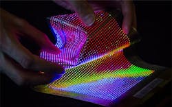
4 Wearable photonics. Wearable photonic technology, which has also been discussed for years, is advancing. Wearable photonics can display information, track personal fitness or medical parameters, serve as a fashion statement, or aid safety at night or in high-radiation environments. It may not be well known that wearable photonics is a prime application for microLEDs, which can be integrated into flexible fabric (see Fig. 1). And, of course, virtual/augmented reality (AR/VR) hardware and software development is spurring innovative approaches to ultralight eyeglass-style displays using waveguide-based and holographic optics. (See “Photonics gets up close and personal: Advancing wearable technology with light,” February 2018 issue; http://bit.ly/2018techreview4.)
Leading-edge photonic components
5 Silicon photonics. Silicon photonic circuits with complete active systems (light sources, intermediate components, and photodetectors) are complex beasts. Because it is very difficult to make silicon emit light at reasonably high levels, such photonic circuits are usually of hybrid construction, with a light source made of III-V semiconductor materials precisely positioned and fixed to the silicon circuit. To combat this complexity, researchers at Fudan University (Shanghai, China) have created an optically pumped all-silicon laser based on silicon nanocrystals and an optimized distributed feedback (DFB) cavity that has the potential, with further development, to be used in silicon photonics. (See “All-silicon laser achieves high optical gain,” April 2018 issue; http://bit.ly/2018techreview5.)
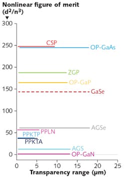
6 Mid-IR optical materials. Coherent infrared (IR) sources often require components made of nonlinear optical materials to achieve a desired wavelength. Engineers at BAE Systems (Nashua, NH) are expanding the utility of such components by working with a wide variety of new mid-IR nonlinear materials (see Fig. 2), many of them patterned or otherwise structured, that can achieve longer-wave IR output using near-IR wavelengths as input. The low-loss, high-figure-of-merit crystals have very large spectral transparency regions that greatly expand the wavelength coverage of highly engineered laser sources. New approaches to fabrication of these crystals are as important as the materials themselves. (See “New materials extend laser spectral coverage deep into the infrared,” April 2018 issue; http://bit.ly/2018techreview6.)7 Flat metasurface lens. By now, the Laser Focus World audience is quite familiar with metasurface optics, which derive their optical capabilities from slowly varying almost-periodic nanostructures fabricated on a usually flat optical substrate, rather than by polished and ground surfaces. As demonstrated often by Federico Capasso’s lab at Harvard University (Cambridge, MA), one metasurface lens can replace multiple conventional optical elements for some purposes. This year, researchers at the Data Storage Institute (Agency for Science, Technology and Research, A*STAR) and Nanyang Technological University (both in Singapore) demonstrated a flat metasurface lens with a numerical aperture (NA) of 0.99 at a 715 nm wavelength. (See “Metamaterial lens has numerical aperture of 0.99,” May 2018 issue; http://bit.ly/2018techreview7.)
8 Ultrafast graphene photodetector. Used in photodetection, graphene has a spectral sensitivity that spans 0.6 to 20 μm, far greater than that of any conventional semiconductor detector material. Unfortunately, graphene’s absorption is only about 2% across that whole range. A group at the University of California Los Angeles (UCLA) has boosted the absorption of a graphene photodetector by forming the materials into nanostripes connected to patches of gold. The resulting device has ultrafast detection capability of up to 50 GHz—with future improvements, this speed could be raised to 425 GHz. (See “Graphene photodetector has 50 GHz speed and high responsivity from 0.6 to 20 μm,” August 2018 issue; http://bit.ly/2018techreview8.)
Ingenious instruments
9 Simple shearing interferometer. While the spatial information in continuous-wave (CW) laser beams can be measured easily enough using a shearing interferometer, where the test wavefront is interfered with a positionally shifted duplicate of itself, this is difficult to do if the laser under test is a femtosecond laser, as the nonzero path length of a typical shearing interferometer prevents the two resulting pulses from interfering. Chunlei Guo and Billy Lam of the University of Rochester (Rochester, NY) have created a simple shearing interferometer with an almost-zero path-length difference that allows even femtosecond pulses to be spatially characterized (the experimental device measured pulses only 65 fs in duration). (See “Simple shearing interferometer measures wavefront of femtosecond laser pulses,” August 2018 issue; http://bit.ly/2018techreview9.)
10 Chip-based spectrometer. Spectrometers are widely used in sensing, materials analysis, optical coherence tomography in medical imaging, and monitoring the performance of optical networks. While smaller spectrometers would lead to wider application, shrinking down a conventional spectrometer results in a reduction of its sensitivity. Researchers at the Massachusetts Institute of Technology (MIT; Cambridge, MA) have found their way around this problem by making a chip-based spectrometer (using standard chipmaking processes) that contains on-chip interferometers with optical switches on each arm that direct light to waveguides of different and unique path lengths, scaled in powers of 2. As a result, the channel count scales exponentially with the number of optical switches—for example, 10 switches produce 1024 channels. See “MIT develops low-cost on-chip optical spectrometers with high channel count and signal-to-noise ratio,” Laser Focus World online; http://bit.ly/2018techreview10.)
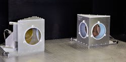
11 High-power laser beam measurement methods. Conventional ways of measuring the power of a laser beam work via absorption of the beam. This works well for low-power beams, but very powerful beams can damage a laser power meter unless heat transfer from the meter is handled very competently. An alternate approach pioneered by the National Institute of Standards and Technology (NIST; Boulder, CO) works by measuring the radiation pressure produced by the beam on a mirror (see Fig. 3)—an approach that gets easier as the beam power goes up. NIST has tested its radiation-pressure laser power meter with 20 kW beams in a manufacturing environment and with a 50 kW beam at the U.S. Army’s High Energy Laser Systems Test Facility (HELSTF; White Sands Missile Range, NM). (See “NIST tests radiation-pressure laser power meter in manufacturing environment,” January 2018 issue, http://bit.ly/2018techreview11 and “NIST tests its radiation-pressure power meter (RPPM) with a 50 kW laser,” June 2018 issue, http://bit.ly/2018techreview12.)Bio-optics with new capabilities
12 Deep learning. Using deep learning, an optical microscope’s performance can be boosted without making changes to its hardware or design, as demonstrated by researchers at UCLA. A deep convolutional neural network (CNN) consisting of stacked layers of artificial neural networks is trained to relate low- and high-resolution images. After training, lower-resolution image data captured by a microscope can be processed by the CNN to improve the image’s resolution. In an experiment, the CNN was trained with a lung-tissue model and tested on breast and kidney tissue—the result was resolution of a spatial period of 0.345 μm. (See “Deep learning improves microscopy images—without system adjustments,” January 2018 issue; http://bit.ly/2018techreview13.)
13 Window to the brain. Optical microscopy techniques to study the brain—for example, two-photon microscopy—would be far more versatile if a noninvasive window to a living brain could be created. Researchers at the Huazhong University of Science and Technology (Wuhan, China) have done just that, increasing skull transparency in mice by using clearing agents—collagenase and glycerol for young mice, and EDTA disodium and glycerol for older mice with higher bone mass. The technique allows imaging of the mouse brain’s cortical structures at synaptic resolution. (See “Noninvasive optical window created in the skull allows brain imaging,” Laser Focus World online; http://bit.ly/2018techreview14.)
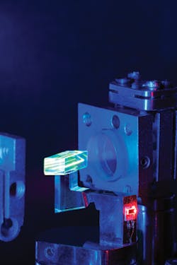
14 Real-time biopsy. In another endeavor to analyze tissue in situ, for example, during endoscopic probing with the desire to do real-time biopsy, researchers at the Institut Fresnel (Marseille, France) are using imaging that includes optical sectioning (that is, 3D imaging), which potentially will allow intraoperative label-free imaging for real-time histopathology diagnosis. The multimodal nonlinear imaging approach uses two-photon autofluorescence (TPF) excitation, second-harmonic generation (SHG), and stimulated Raman to image cell bodies, their nuclei, and the extracellular matrix. A hollow-core fiber with a glass microsphere at the end produces a spot that is scanned via a piezo actuator (see Fig. 4). The multimodal endoscope was shown to reveal the complex morphological structure of human tissue. (See “Multimodal endoscopy targets real-time biopsy,” June 2018 issue; http://bit.ly/2018techreview15.)15 Several-trillion-frames-per-second camera. Biomedicine is currently hampered by the fact that living tissue is a dynamic scattering medium with speckle decorrelation on the order of milliseconds. Scientists at the California Institute of Technology (Caltech; Pasadena, CA) and the Director of Caltech Optical Imaging Laboratory (COIL, also in Pasadena) are using a variation of single-shot compressed ultrafast photography (CUP), which they call T-CUP, to perform femtosecond imaging of transient light patterns in in vivo tissue in single exposures. Image data acquired by a femtosecond streak camera is subjected to a so-called radon transformation to obtain a high-quality image; recording rates range from single-shot to 10 trillion frames per second. (See “Real-time 10 trillion frames/s camera will facilitate in vivo imaging,” November 2018 issue; http://bit.ly/2018techreview16.)
Novel applications
16 All-optical cryogenic cooling. Cryocoolers are often used to cool IR detectors to reduce their signal-to-noise ratio. While a dewar filled with liquid nitrogen can cool a detector for a short time, remote applications usually rely on a mechanical cryocooler—which itself is a source of signal degradation in the form of mechanical vibration. Researchers at Los Alamos National Laboratory (Los Alamos, NM) and the University of New Mexico (Albuquerque, NM) have now demonstrated an all-optical cryogenic cooler that has no moving parts and thus no vibration. A laser cools a ytterbium-doped fluoride crystal via fluorescence excitation, producing a loss of energy from the crystal; in an experiment, a mercury cadmium telluride (HgCdTe) optical sensor was kept at a temperature of 134.9 K (see Fig. 5). Uses include space-based sensing. (See “All-optical cryogenic cooling of sensors eliminates vibration,” July 2018 issue; http://bit.ly/2018techreview17.)17 High-power blue laser. Laser welding of copper is becoming widespread in the manufacture of lithium-ion batteries, but the near-IR wavelengths of most industrial lasers are poorly absorbed by copper. High-power green lasers have been developed to take advantage of copper’s increased absorptance at that wavelength—however, blue light is absorbed even better. Now, Nuburu (Centennial, CO) has commercially introduced a high-power blue direct-diode (laser diodes coupled into fiber) laser system for copper welding. The 150 W system has demonstrated void- and spatter-free welding of 40 10-µm-thick copper foils, and a 500 W system is due out soon. (See “Blue direct-diode lasers extend industrial laser capability,” September 2018 issue; http://bit.ly/2018techreview18.)
18 Terabit-per-second data transmission over optical fiber. The transmission of data over optical fiber has reached well into the terabit-per-second region. Now, a group at the National Institute of Information and Communications Technology (NICT) and Fujikura (both in Tokyo, Japan) has demonstrated the transmission of 159 Tbit/s of data over a 1045 km distance using a three-mode optical fiber. Mode multiplexing was used in combination with 16-QAM (quadrature-amplitude modulation), which is a practical high-density multilevel modulation optical signal, for all 348 wavelengths—multiple-input and multiple-output (MIMO) enables unscrambling of mixed modal signals even after transmission over more than 1000 km. Because the three-mode optical fiber has a standard 125 µm outer diameter, it can be cabled using existing equipment. (See “NICT researchers show world-record 159 Tbit/s transmission over 1045 km with three-mode optical fiber,” Laser Focus World online; http://bit.ly/2018techreview19.)
19 Shaped femtosecond laser pulses. Ultrafast lasers have made their way into the materials-processing world, producing pulses that ablate rather than melt substances and resulting in little or no cratering or debris. Scientists at the Beijing Institute of Technology (Beijing, China), the University of Minnesota (Minneapolis, MN), and the University of Nebraska-Lincoln are now shaping femtosecond laser pulses to improve the quality of the ultrafast microfabrication process and are extensively computer-modeling these processes. The researchers experimented with temporally and spatially shaping femtosecond pulses, creating subpulses that have a pulse delay shorter than the characteristic time scale of electron-lattice coupling. Many very large benefits ensued: in just one example, the processing efficiency of microchannel fabrication was increased by 56X and the maximum aspect ratio of the microchannels increased by 3X. (See “Shaped femtosecond laser pulses alter electron dynamics to improve ultrafast-laser micromachining quality,” Laser Focus World online; http://bit.ly/2018techreview20.)
20 Efficient microscale nuclear fusion. Microscale laser-initiated nuclear fusion in the lab, achieved by scientists at Colorado State University (CSU; Fort Collins, CO), can potentially lead to advances in neutron-based imaging and neutron probes to gain insight on the structure and properties of materials. The researchers focused pulses with 60 fs duration, energies up to 1.65 J, and a center wavelength of 400 nm onto an array of 200- or 400-nm-diameter deuterated polyethylene (CD2) nanowires, producing deuteron-deuteron (D-D) fusion. The maximum number of neutrons per shot was about 3.6 × 10⁶ for a laser pulse energy of 1.64 J, corresponding to 2.2 × 10⁶ neutrons per joule. (See “Laser-heated nanowires produce microscale nuclear fusion with record efficiency,” April 2018 issue; http://bit.ly/2018techreview21.)
About the Author
John Wallace
Senior Technical Editor (1998-2022)
John Wallace was with Laser Focus World for nearly 25 years, retiring in late June 2022. He obtained a bachelor's degree in mechanical engineering and physics at Rutgers University and a master's in optical engineering at the University of Rochester. Before becoming an editor, John worked as an engineer at RCA, Exxon, Eastman Kodak, and GCA Corporation.


