Optical Design Software: Numerical analysis enables energy-efficient photonic switches
DRITAN CELO, ERIC BERNIER, and DOMINIC GOODWILL
All-optical networks were envisioned decades ago because of their potential for high transmission speeds, thus satisfying ever-increasing demands on network performance. Photonic switches are already widely deployed throughout cities and long-distance networks, while experiments in data centers and with high-performance computing are ongoing. Huawei Technologies Canada (Markham, ON, Canada) is radically improving critical optical components, such as photonic switches, using silicon photonics (SiPh).
To route data at various points in an optical network, the optical signal is traditionally converted back to an electrical signal, switched, and then converted again to an optical signal. Converting the signal uses large, power-hungry equipment, which adds latency while each packet is converted. In comparison, photonic switches do not convert the signal format, so they are often faster, smaller, and more energy-efficient.
Existing photonic switches, however, are bulky, expensive, and made of many hand-assembled components. To address the issue, Huawei is developing circuits using integrated SiPh technology. Optical circuits are made in CMOS chip foundries and contain Si waveguides about 0.5 µm across, which is possible because Si is transparent at the signal wavelengths.
Engineers at Huawei are prototyping some of the most complex SiPh circuits in the world, relying on an integrated design environment. Highly accurate numerical physics models are fine-tuned through iterative prototyping cycles, while photonic-circuit layout software ensures first-time-right chip design. The thermal performance of the thermo-optic SiPh switch is a core part of this design workflow.
Thermo-optic switches based on phase shift
The thermo-optic switch under development is a silicon photonic Mach-Zehnder (MZ) interferometer, which has two states: a “cross” state and a “bar” state. By default, the MZ is in the cross state (see Fig. 1). A light wave arriving at an input (for example, input 1) is split and travels along both arms. The light from the two arms interferes at the output coupler. Because of the relative phase of the light from the two arms, all the light exits from output 2.
A thermally induced phase shift provides a way to flip the switch state. To switch a thermo-optic MZ to its bar state, one arm of the MZ is heated. This changes the refractive index of the waveguide, creating a π phase shift in the light propagating in that arm. Interference causes the light to exit from output 1, carrying data toward a different destination. By combining a large number of these switch cells on one chip, a large switch matrix is created.
Thermal analysis and design optimization
The requirements on power consumption, switching speed, and physical size, together with the manufacturing design rules of the thermal undercut, combine to create a significant optimization problem for the implementation of thermo-optic MZ switches. To arrive at a final design, thermal analysis in COMSOL Multiphysics software provides an efficient means for Huawei to quantitatively evaluate new designs before manufacturing physical prototypes.
For example, thermal analysis is used to quantify the performance of different thermo-optic designs, both with and without thermal undercut, which is an important consideration since undercut adds additional steps to the manufacturing process. While using a thermal undercut can improve the energy efficiency of a device, there is a decrease in switching speed, so a device geometry with undercut is suited only for certain applications.
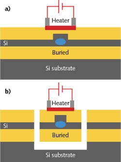
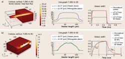
The device geometry (see Fig. 2) was implemented in COMSOL software, both with and without using a thermal undercut. To reduce the computation time required for steady state thermal analysis of each design, half symmetry was used as indicated by the dashed black line, and the resulting model geometry is shown at left in Figure 4. Silicon waveguides that are hundreds of micrometers in length are buried in silica glass on top of a silicon substrate. Material properties assigned to each domain in the model were chosen from options that are already available in the software. Since SiPh structures have high-aspect ratios of 1000:1, COMSOL Multiphysics meshing algorithms were critical for fast and accurate modeling.Heat transfer in solids is modeled throughout the device geometry, with insulating boundary conditions defined on the surface passivation layer and thermal undercut boundaries when present. The TiN heater in the heated waveguide arm is defined as the heat source in the switch model, and simulation results reveal how much applied thermal power is required to produce a π phase shift for a given design. To produce a π phase shift, the waveguide temperature must change by 13.3 K, which is a value determined from optical test measurements.
Steady-state analysis of the thermo-optic SiPh switch demonstrates a 23X reduction in the amount of power required to achieve a π phase shift when a thermal undercut is included in the design. The temperature distribution is shown at left in Figure 4 for each device geometry. The plots in the middle depict the temperature difference between the heater and waveguide, demonstrating the extent of heat loss to the surrounding materials in devices without undercut.
A difference of 0.2 K was achieved in the design with undercut, compared to a 13 K difference without. Transient analysis, using quarter symmetry to further reduce computation time, provides information on how long it takes to tune the waveguide to the desired temperature and phase, which limits the cross/bar switching speed of the device.
Although devices with undercut are more energy-efficient, they do not tune as quickly as devices without undercut, as demonstrated by the rise and fall times at right in Figure 4. The validated steady state and transient models are also critical for evaluating the thickness of the silica glass, overall size of an individual MZ switch, and effect of a cooling passivation layer on top of the device, thus enabling an application to maximally benefit from reduced power consumption.
Thousands of switches on a single chip
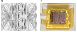
Although the focus of the heat transfer simulations is to optimize a single thermo-optic MZ switch, in actual practice, they are not found alone, but used in large switching matrices (see Fig. 5). Huawei’s matrix is designed to prevent optical crosstalk, which ensures that the optical signals out of the switch are very clean.The architecture at left represents a 32 × 32 SiPh switch matrix containing 448 2 × 2 thermo-optic MZ switch cells. A light path passes through one cell in each column, and the path is defined by applying the appropriate cross or bar drive power to those cells. Supplying power to a switch raises the underlying waveguide temperate and generates the necessary π phase shift that allows a signal to propagate along a chosen path.
Entering the prototyping and large-scale product development phase opens up new challenges, which require designers to divide their time between the R&D facilities at Huawei and the foundry. Thermal performance is a small, but important piece of the very large puzzle that represents the device design workflow. Looking toward large-scale product development, fabricating a 128 × 128 SiPh switch with thousands of MZ cells on a single die that consumes no more than 50 W of power, which may be used in many different environments, raises questions about mechanical stability. Structural analysis of the packaged switch has now become a focus, and numerical simulation in COMSOL software will again prove useful to optimize its design.
REFERENCES
1. D. Celo et al., “32x32 silicon photonic switch,” Optoelectronics and Communications Conference/International Conference on Photonics in Switching, Niigata, Japan (2016).
2. D. Celo et al., “Thermo-optic silicon photonics with low power and extreme resilience to over-drive,” IEEE Optical Interconnects Conference, San Diego, CA (2016); doi:10.1109/oic.2016.7482994.
Dritan Celo is a senior engineer, Eric Bernier is leader of advanced photonics, and Dominic Goodwill is a senior principal engineer, all at Huawei Technologies Canada, Markham, ON, Canada; e-mail: [email protected]; www.huawei.com/ca.


