INTEGRATED OPTICS: Simulation and design tools address demands of WDM
MARTIN AMERSFOORT
In the last few years, optical networks using multiple wavelengths to transmit data through optical fibers have become a significant commercial success. Whereas the initial implementations were concerned with simple point-to-point long-distance links, WDM is likely to enter more-complex network topologies with increased penetration into metropolitan and local networks. In addition, the number of wavelengths transmitted over a single fiber has increased dramatically. The continuing call for higher bandwidth has created a huge demand for a variety of optical components. Due to their compactness, robustness, and suitability to large-scale production, optoelectronic integrated circuits (OEICs) that combine a number of elements on a single chip will play an important role in satisfying this demand.
Optoelectronic integrated-circuit technology is based on the waveguide properties of channels (or shaped layers) of material with refractive indexes higher than the surrounding media. Total reflection of light on the interfaces of these channels and on adjacent materials enables light propagation through certain paths (analogous to light propagation in fibers) and opens possibilities for the construction of optical circuits. Computer-aided-design (CAD) tools will play a paramount role in reducing the time-to-market of these components. In this article we present an overview of the most commonly used design and simulation tools as well as requirements for a short and efficient design cycle.
Design cycle
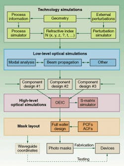
Several elements and steps are involved in a typical OEIC design cycle (see Fig. 1). The central information that determines the performance of a OEIC is the refractive index distribution as a function of the spatial coordinates, wavelength, and other parameters. For a simple step-index etched waveguide structure, this information can be directly obtained from the planar geometry of the chip combined with dispersion models for the materials being used.For other waveguide structures, fabricated by in-diffusion or ion-exchange, full two-dimensional modeling of the in-diffusion process may be required. Also, calculation of the refractive index perturbation due to an externally applied interaction (such as a heater-induced temperature distribution) can be included in this step. Subsequently the refractive index data are used for the simulation and optimization of the optical performance of the basic components that are part of the OEIC.
Due to interference effects inside the waveguides, light cannot propagate in arbitrary ways but instead travels in modes. The modes manifest in distinguishable intensity distributions and phase velocities. For many applications it is essential that the waveguides support only one or at most a few modes. This can be achieved using channels that have dimensions on the order of the wavelength of the light.
Therefore, understanding and controlling the modal properties is of paramount importance for the design of integrated optical circuits. Unfortunately, almost none of the known waveguide geometries allow for an analytical derivation of the mode properties, thus requiring numerical tools (often called mode-solvers). Methods for analysis of modes of straight and curved waveguides range from approximate and scalar methods (such as the effective index method) to full-vectorial approaches (based on finite difference or finite element schemes, for example).
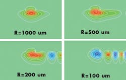
One of the important applications of eigenmode solvers is the calculation of the inherent radiation losses occurring in curved waveguides that interconnect different components on the OEIC. To minimize the size of the OEIC it is important to know the minimum allowable radius of curvature. In the case of a curved ridge waveguide in indium phosphide/indium gallium arsenide phosphide (InP/InGaAsP), the calculated intensity distribution of the eigenmode shows that with decreasing radius of curvature the waveguide becomes more and more leaky, and consequently the radiation losses increase dramatically (see Fig. 2).An alternative popular method for modeling light propagation in OEICs is the beam propagation method (BPM). Due to its straightforward implementation for a large class of waveguide structures, it is used in most (commercial) modeling tools. In BPM, the total optical field is propagated in a stepwise manner through slices of a known waveguide structure. The latest methods are based on finite difference schemes in combination with the so-called slowly varying envelope approximation (SVEA). In the SVEA, the fast phase variations of the optical field due to average propagation velocity are eliminated. The result is a differential equation, which contains only a slowly varying field that is much more suitable to discretization for numerical approximation. Although BPM and eigenmode analyses are clearly different simulation concepts, generally speaking they are used together and integrated in the same design tool.
The simulation methods outlined above are primarily used for modeling components with modest levels of complexity, which is in fact sufficient for the majority of the components being researched and developed today. However as the complexity of OEICs continues to grow, due to integration of more functionality onto a single chip, there will be a need for design tools that can manage this level of complexity. One of the interesting candidates is a scattering matrix approach, pioneered by the Delft University of Technology (Delft, the Netherlands) that divides the structure into blocks. These blocks are described by matrices that quantify the transfer of modes from the input to the output of each block. Simple cascading of the matrices is equivalent to simulating the propagation through the entire structure.
Design tool requirements
The design cycle outlined above is generally not a simple sequential trajectory. At any point in the design cycle, a designer may need to go back one or more steps. This can be the case if the desired device performance cannot be met or leads to unrealistic fabrication tolerances. Alternatively, size limitations encountered during the mask layout stage may require a redesign of the basic OEIC parameters. For these reasons a typical design cycle consists of a large number of individual steps. To achieve a short design cycle, each step must be carried out with minimum effort and smooth transition to other design steps.
This requirement leads to several specific requirements for design tools. First of all they should be parametric. Waveguide dimensions and material parameters should be specified using variables and expressions rather than real numbers, such that modifications (for example the radius of bends) can be incorporated through the entire design within a matter of seconds. To minimize the time required to design and modify more-complex OEICs and their masks, it is important that the tools support a hierarchical design approach. Modifications in the basic parameters should be automatically reflected in the entire design. As pointed out above, a hierarchical approach at the simulation level can reduce simulation times for complex OEICs. Finally, it is important to have a high level of vertical integration between the different design and simulation tools. An example is the integration of the BPM simulator with the mask layout tool, with import and export capabilities to a variety of mask formats (such as GDS2, CIF, and DXF).
Design example
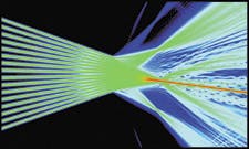
A high-level layout language with BPM capabilities played a central role in the design of a 1 x 8 optical switch at the IBM Research Laboratory in Zürich, Switzerland (see Fig. 3). Researchers used plasma-enhanced chemical vapor deposition to produce low-loss, high-contrast, silicon-oxynitride waveguides. The high contrast enabled small bending radii (R = <1.5 mm) combined with low propagation losses (<0.1 dB/cm).The research team developed a novel switching concept based on thermo-optic beam steering induced by individually addressing heater sections on an array of waveguides. By adjusting the phase distributions over the array waveguides, the researchers targeted a specific output waveguide for refocusing the light. A design package was used to lay out the complex waveguide circuit and to simulate device performance. The purpose was to optimize the design by minimizing the losses and crosstalk occurring in the focal plane of the switch. The isolation of the seven "off" channels relative to the power in the "on" channel of the 1 x 8 switch was measured to be better than 22 dB for devices based on the initial design. (Details are scheduled for publication in Photonics Technology Letters, Nov. 1999).
Martin Amersfoort is general manager of BBV Design, Hengelosestraat 705, 7521 PA, Enschede, the Netherlands; e-mail: [email protected].


