Optical inspection data helps integrate telecom laser-diode production

In the typical manufacturing process, devices are formed by depositing and etching materials on an epitaxial layer of gallium arsenide or indium phosphide. This compound semiconductor substrate is cleaved into bars of 25 to 50 devices, and the bars are stacked in deposition fixtures. The two cleaved surfaces (facets) of the bars are antireflective (AR) or high-reflective (HR) coated to complete the laser cavity. The bars are then diced into individual devices that are mounted, aligned, wire-bonded, and packaged.
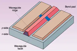
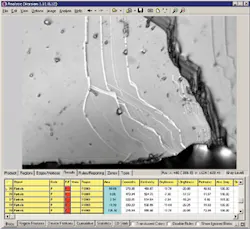
Typically, manual optical inspection has been employed to screen and eliminate damaged devices. Inspections can occur after wafer-level deposition, bar-level AR/HR coating, and final dicing. Defects can include cracks, chips, delamination, or incomplete formation of the waveguide ridge. Other defects could be delamination or coating damage on the facet ends, and cleave deviation due to final dicing (see Fig. 2).The results of manual inspection, however, tend to be highly variable, and subject to the judgment of individual operators, their level of training, and consistency over time. Manual screening eliminates a percentage of defective parts (along with a quantity of good parts), but it does not provide quantitative results that engineers can use to improve processes and prevent further defects. In contrast, automated optical inspection has proven to be a fast and highly repeatable method for capturing surface defects, as well as measuring critical dimensions such as the width and height of the waveguide ridge. Through rules-based analysis of digital images, optical inspection provides nonsubjective, numeric evaluation of device quality that can be used to adjust and improve prior processes (see Fig. 3).
Major software functions
The software that governs automated inspection systems must fill five major needs—a user interface for production control, command of automation, data capture, data analysis, and defect determination. It must also provide an interface with manufacturing data systems and production equipment.
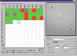
Data analysis is the heart of the software suite. In our "Analyze" defect-inspection software, for example, defects are determined using a rules-based architecture. For each part, a high-resolution image is captured. A template is compared against the image, which is then rotated and translated to match a known reference. Any deviations from the reference (known as "blobs") are tagged. For each blob, the software extracts parameters such as location, size, shape and darkness. The defects are classified based on these parameters; for example, a long, skinny deviation will be considered a crack, while a circular mass may be classified as contamination. The software then employs user-defined rules to determine whether the defects, singularly or collectively, are significant enough to fail the part. Finally, the results are recorded to a text file for use in parts tracking and/or statistical process control.
The benefits of rules-based software architecture are twofold. For one, rules allow the software to be tailored to a particular application, providing pertinent, numeric quality assessments. Second, the process of setting up rules requires developers to carefully consider which defects may be present and how they affect part performance. The nonsubjective, highly repeatable data allow process developers to establish meaningful, effective quality levels at each process.
Taken a step further, optical inspection data can be used to track quality throughout the process. Manufacturers are implementing bar- and device-level serialization so that inspection data can be tied to particular parts and tracked. Automated inspection stations, using the same software and protocols, are being employed at all inspection steps, allowing data to be correlated from wafer to bar to die levels. In this manner, early part conditions can be correlated with final performance, such that realistic, cost-appropriate process controls can be established.
Increasing yield
Manual handling of parts is widely recognized as a prime source of yield loss. To address the problem, manufacturers have focused on automating labor-intensive inspection and handling operations. Pick and place automation is being implemented to stack bars into deposition jigs prior to AR coating, to unstack after this step, and to handle individual bars and dies prior to final inspection.
By incorporating optical-inspection data, this same equipment can be used to sort serialized bars or dies, removing defective parts automatically and improving throughput at subsequent processes. This arrangement also helps ensure data integrity by automatically tying all data to the appropriate dies, without the need for manual tracking. Further throughput gains are being sought by combining automated inspections. Through innovative tooling, bar-level inspection of the epi (waveguide) and facet surfaces can be accomplished at a single optical inspection station.
With process equipment, automation, and metrology equipment unified by data, the next logical step will be to combine the physical equipment into functional stations. Active device manufacturers have already begun to employ cluster tools that complete multiple deposition and etch operations without breaking vacuum. Process developers will also likely begin to deploy in situ metrology and integrated automation as well. Because component manufacturers face a wide range of structures, materials, and equipment platforms, developers may find that "islands of automation" prove more effective than the "automated fab" goals of the more standardized semiconductor industry.
Standards, and standards-generating bodies, will need to be developed for component manufacturing as well. The difficulties here are compounded by the disparity and large quantity of optical devices being rapidly developed. The onus will rest, in part, on metrology manufacturers, to provide guidance and leadership for inspection standards and data-handling protocols.
About the Author
Mike Zecchino
Technical Communications, 4D Technology
Mike Zecchino is in technical communications at 4D Technology, Tucson, AZ.

