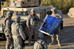
Holographic maps developed by Zebra Imaging (Austin, TX) and sponsored by a US Army contract allow soldiers to view three-dimensional (3D) landscapes and cityscapes prior to entering a battle zone. The technology, which has other uses in both military and civilian applications, relies on software that converts light detection and ranging (lidar) data into an up to 24 × 36 sq-in. rollable laser-written holographic display that can be observed using a simple flashlight, without the need for special viewing glasses or goggles. As the display is moved, 3D details of the scene can be observed from different angles, with a perceived depth up to 30 cm.
The full-parallax 3D display allows groups of individuals to view the map simultaneously, providing a crucial advantage on the battlefield for soldiers in unfamiliar terrain. The laser-written maps, created from open-source images and lidar data, can be produced in just a few hours and shipped to the field in 7–10 days. To date, around 13,000 of the maps have been deployed for combat use. Born out of a Defense Advanced Research Projects Agency (DARPA; Arlington, VA) program, Zebra Imaging is now working on a dynamic display that would use satellite imagery to update the display in near real time. Contact Eric Doane at edoane@zebraimaging.com.

Gail Overton | Senior Editor (2004-2020)
Gail has more than 30 years of engineering, marketing, product management, and editorial experience in the photonics and optical communications industry. Before joining the staff at Laser Focus World in 2004, she held many product management and product marketing roles in the fiber-optics industry, most notably at Hughes (El Segundo, CA), GTE Labs (Waltham, MA), Corning (Corning, NY), Photon Kinetics (Beaverton, OR), and Newport Corporation (Irvine, CA). During her marketing career, Gail published articles in WDM Solutions and Sensors magazine and traveled internationally to conduct product and sales training. Gail received her BS degree in physics, with an emphasis in optics, from San Diego State University in San Diego, CA in May 1986.
