Image-processing-based modular inspection system works from macroscopic to microscopic levels
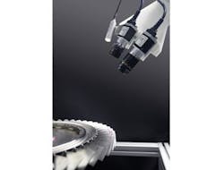
For better quality control of component surfaces, researchers at the Fraunhofer Institute for Industrial Mathematics ITWM (Kaiserslautern, Germany) have created a high-precision modular inspection system that can be adapted on a customer-specific basis and integrated into a production process.
To check a component in, for example, an automotive or aerospace assembly line, manufacturers apply image-processing methods. Multiple cameras take pictures of component surfaces from various angles, which are analyzed by software. "Every material substance has its own unique surface structure," says Markus Rauhut of the Fraunhofer Institute for Industrial Mathematics ITWM. "To evaluate its quality, the testing procedure has to be gauged precisely to these specific properties."
The size and shape of a component play a role, as well as the desired resolution of the images. Even though there is an array of surface inspection systems already on the market, they are only configured for specific materials and dimensions. Standard solutions cannot cover the entire spectrum of possible testing needs.
Modifiable MASC
In response, the researchers at ITWM have engineered a modular inspection system they have dubbed Modular Algorithms for Surface InspeCtion (MASC), which can be modified to customer-defined specifications. "Our system is suited for the most diverse materials—like metals, leather, textiles or paper—and covers a size range from tiny components for medical technology through to entire sheets of rawhide or ceiling panels," says Rauhut.
First, the surface of the workpiece is illuminated and scanned using multiple cameras set at a wide range of angles. With free-form surfaces, regions that are covered by curvatures or corners are also recorded in this manner. The more complex the geometry, the more cameras are needed, as a rule. The scientists developed mathematical evaluation algorithms and have built up a comprehensive software library. "For instance, one algorithm is programmed to find edges or certain color points in the image," says Kai Taeubner of ITWM.
Algorithms work at the microscopic level
One particular challenge includes those inspection procedures that require very high resolution. No surface is quite homogeneous; indeed, they feature small scratches or fluctuations in brightness. For projects where resolution reaches the microscopic level, it becomes increasingly difficult to differentiate between anomalies in the surface texture and actual defects. The consequence: components that are actually free of defects get sorted out as defective. "That is another advantage of our procedure: With the aid of our algorithms, we can refine the analysis to such a degree that incorrectly identified flaws become virtually eliminated," says Taeubner.
Once all testing parameters are set, the procedure is integrated into the production process with the customer. The cameras are either installed directly on the assembly line, or are held and moved about by robots. When a defect is found, the production process automatically stops; at the same time, the machine operator is notified. The detected defects are classified and the test object is sorted into a particular quality class.
Source: http://www.fraunhofer.de/en/press/research-news/2014/august/customized-surface-inspection.html

John Wallace | Senior Technical Editor (1998-2022)
John Wallace was with Laser Focus World for nearly 25 years, retiring in late June 2022. He obtained a bachelor's degree in mechanical engineering and physics at Rutgers University and a master's in optical engineering at the University of Rochester. Before becoming an editor, John worked as an engineer at RCA, Exxon, Eastman Kodak, and GCA Corporation.
