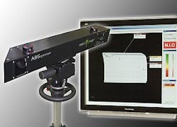
Surface testing from Steinbichler Optotechnik uses a blue LED
The ABIS optimizer portable surface testing system provides both depth and objective surface evaluation. The compact, robust device includes dust-proof optical components and uses a blue LED. It allows partial focus area examinations of a defect region during manufacturing.
Steinbichler Optotechnik
Neubeuern, Germany
-----
PRESS RELEASE
Steinbichler Optotechnik presents a portable surface testing system ABIS optimizer and new T-SCAN sensor at the CONTROL trade fair
Steinbichler Optotechnik GmbH from Neubeuern, the worldwide leading supplier of optical measuring and sensor technology, will present two innovative new products at the CONTROL 2012 trade fair (hall 5 stand 5304): the STEINBICHLER ABIS optimizer, the world's first portable surface testing system with depth evaluation and an objective surface evaluation as well as the STEINBICHLER T-SCAN, a new laser scanner with a considerably improved performance. "The ABIS optimizer – a logical further development from the numerous automatic ABIS systems already used on the market – is especially developed for applications at an extremely early stage of the manufacturing process and is consistently equipped with all of the necessary technical features required for this. The new T-SCAN, on the other hand, offers a data transfer rate which is up to 30 times higher than its predecessor and achieves a previously unseen performance thanks to its larger line thickness and a higher stand-off,“ reports Hans Weigert, Head of Sales/Marketing at the Steinbichler Optotechnik GmbH.
Due to its extremely compact construction and the user-friendly arrangement of all additional components such as the power supply and the USB port to the laptop, STEINBICHLER ABIS optimizer is intended to be operated in an error-free way by all users from the production environment, all the more so as the robust construction and the dustproof optical components of the system enable it to be used in the most difficult of industrial conditions. The use of the BLUE LED technology combined with the completely revised technical design opens up optimal areas of application, in particular in tool design and construction, of the pilot production and during the entire optimisation process.
STEINBICHER ABIS optimizer applies already at a very early stage of the manufacturing process in order to avoid costly subsequent work in good time. Partial focus area examinations of a defect region during manufacturing and the supporting of virtually all surface quality areas no longer pose a problem with the system. Last but not least, thanks to its excellent price/performance ratio, the surface testing system is the perfect tool for always conveying and also tracking an objective and reproducible impression of the surface quality with regard to its dents, distortion, rippling and other abnormalities during the tool design and construction and also during the entire process chain.
As a result of its large dynamic range on the most varied of surfaces, T-SCAN enables better measuring results than its predecessor the T-SCAN 3. Together with the new Steinbichler tracking system which has also been especially developed for the sensor, customers receive a directly harmonised, holistic solution. Compared to technologies such as index arms and coordinating machines, the new laser scanner offers a considerable advantage thanks to the dynamic referencing alone which also enables work to be carried out even in oscillating or moving environments without loss of precision.
"This year, our CONTROL appearance will be marked by the 25 year company anniversary of Steinbichler Optotechnik. For a quarter of a century, we have made an important contribution to the further development of measuring and sensor technology with product innovations and our constantly growing team, now entailing 160 members of staff. This competence – which is now expected of Steinbichler Optotechnik by our customers – has also, of course, influenced the STEINBICHLER ABIS optimizer and the STEINBICHLER T-SCAN,“ says Hans Weigert who is pleased to be able to present two important new products at the CONTROL trade fair in the company's anniversary year.
Steinbichler Optotechnik GmbH is well-known around the world for its years of expertise in high-precision optical measurement and sensor technology as well as for efficient hardware and software solutions designed primarily around the needs of the automotive, aerospace and tire industries. Founded in 1987 and headquartered in Neubeuern, Germany, the international company today has a staff of 200 employees. In addition to a worldwide distributor network, Steinbichler has subsidiaries in the USA, Brazil, China, India and Portugal. Reference customers include Airbus, Audi, BMW, Boeing, Daimler, EADS, Siemens, Sony and Thyssen. Further information about Steinbichler Optotechnik is available on our website at www.steinbichler.com.
-----
Follow Laser Focus World on your iPhone or Android
Subscribe now to Laser Focus World magazine; it's free!
