3D optical interferometry with True Color visualization advances understanding of flexible electronics
KURT A. RUBIN, RAYNER SCHELWALD, DIMITRIS BARMPAKOS, APOSTOLOS SEGKOS, CHRISTOS TSAMIS, and GRIGORIS KALTSAS
3D optical profiling is a noncontact, high-resolution measurement and visualization technique used to measure the topography and geometry of devices and materials.1, 2 Capabilities of commercial 3D interferometry systems have steadily improved; today, they can measure vertical nano- and microtopography spanning Ångstroms to many millimeters in length scale. True Color imaging, developed by KLA, provides additional understanding that is complimentary to topography. Advances in optomechanical hardware, optics, electronics, and software now make it possible to create economical precision 3D interferometric measurement systems, enabling 3D profiling to help a broader range of industrial and scientific applications.
This article provides an example of how the capabilities of this new generation of 3D optical measurements can be applied to the fields of printed and flexible electronics. Flexible electronics is characterized by a rich and diverse set of functions, device topographies, fabrication technologies, and various materials (conducting, insulating, dielectric, etc.), which have complex surface structures with diverse optical properties. Multiparameter printed arrays on flexible substrates can be used for sensing humidity, temperature, and mechanical strain, as well as for thermoelectric generators and many other purposes, all of which have performance dependencies upon geometry and fabrication process.3
Experimental method and results
Figure 1a is an example of an economical integrated 3D interferometric optical profiler platform incorporating white-light interferometry (WLI), phase-shift interferometry (PSI), True Color imaging, and stitching. Figure 1b is a schematic layout of the interferometric system; it incorporates a broadband white-light source and Mirau interference objective lenses to perform WLI, PSI, and composite WLI + PSI. Interference of light reflected from the sample and the internal Mirau reference mirror gives rise to topography-dependent interference patterns, which are captured by a high-resolution camera and converted into 3D topographic data. True Color information about the sample coloring is also acquired as a function of topographic height.
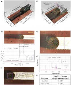
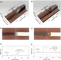
Figure 2 provides an example of measurements of a prototype flexible electronic device fabricated using multilayer inkjet printing of two different materials on a flexible polyamide substrate.5, 6 The 3D images in this article were analyzed within the Profilm analysis environment and are available to the reader.7 The devices are 3D composite structures built entirely by multilayer inkjet printing. Electrical contacts were formed by inkjet printing slightly overlapping 80-μm-diameter drops filled with concentrated ~100-nm-diameter silver (Ag) nanoparticles. Conductor traces were formed by inkjet-printing organic PEDOT:PSS mixed with various wt% carbon quantum dots (CQDs), partially overlapping previously inkjet-printed Ag-nanoparticle contacts. PEDOT:PSS is a semitransparent material in a class of electrically conducting polymers used for conductive wearable flexible fabrics, sensing, and functional electronics. CQDs enhance and enable tunability of the electrical conductivity and optical response of PEDOT:PSS. The topography of inkjet-deposited materials can be affected by solvents that evaporate, so topographic and True Color measurements make it possible to quickly characterize the printed devices’ geometries and connect the optical color to the fabrication process.
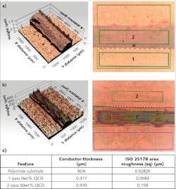
Modern interferometers can measure the topography of samples with a wide range of lateral physical and vertical size. Figure 2a-g illustrates the 3D topography and True Color of a device in which an array of separate field-of-view data acquired with a 10X objective were stitched together to form a single composite image encompassing the full device area. The 3D plots have height and True Color plotted together. Figure 2a-c illustrates 3D topography and True Color of a two-pass inkjet-printed conductor trace partially overlapping an Ag electrical contact. The contact, which is built up from printing layers of Ag nanoparticles, exhibits macroscale roughness, including deep trenches and steep sidewalls after solvent from the deposition process evaporates. WLI is able to measure the depth of the bottom of the trenches and characterize the heights of the sidewall geometries. Figures 2c and 2h illustrate how the PEDOT:PSS material makes electrical contact by overcoating the Ag contact and reduces surface roughness by ~20% by partially planarizing the overlap region of the device. True Color allows different materials and regions to be clearly differentiated. Topographic, geometric, and color information guides improvements to the fabrication process and modeling to improve device geometry and performance.Outlook
The True Color and topographic measurement examples discussed here for printed flexible electronics can be applied to other fields requiring understanding of the interplay of topography and geometry with process development, fabrication, materials, and performance. Recent technical advances have made 3D optical interferometers more economical while maintaining their ability to precisely measure small height features. Interferometric optical profilers measure topography spanning millimeter to Ångstrom heights using white-light and phase-shifting interferometry. Topography and True Color data provide complementary information about geometry and material. 3D optical interferometry is used to characterize established and emerging devices and materials in industrial and scientific applications including optics, solar, LEDs, laser processing, semiconductors, microfluidics, MEMS, 3D printing, and etching and deposition. 3D optical profiling is routinely used for inspection, failure analysis, metrology, defect analysis, and roughness and step-height measurements.
ACKNOWLEDGEMENTS
KLA and Filmetrics are registered trademarks of KLA Corporation.
REFERENCES
1. M. Quinten, A Practical Guide to Surface Metrology, Springer (2019).
2. T. Yoshizawa, Handbook of Optical Metrology, Principles and Applications, second edition, CRC Press (2017).
3. S. Khan et al., IEEE Sens. J., 15, 3164–3185 (Jun. 2015).
4. See http://bit.ly/KLARef4.
5. D. Barmpakos et al., Microelectron. Eng., vol.225, C, 111266 (2020).
6. D. Barmpakos et al., Transducers 2019 – EuroSensors XXXIII, 2515 (2019).
7. See http://bit.ly/KLARef7.
Kurt A. Rubin is with KLA Corporation, Milpitas, CA; Rayner Schelwald is with Filmetrics, a KLA Company, Unterhaching, Germany; Dimitris Barmpakos and Grigoris Kaltsas are with the microSENSES Laboratory in the Department of Electrical and Electronic Engineering at the University of West Attica, Athens, Greece, and Dimitris Barmpakos, Apostolos Segkos, and Christos Tsamis are with the Institute of Nanoscience and Nanotechnology at the National Centre for Scientific Research “Demokritos,” Athens, Greece; e-mail: [email protected]; kla.com.
![FIGURE 1. The compact 3D interferometric optical profiler is shown (a) [4]; the x-y stage positions the sample and tilts in two directions to align the sample to the objective lens axis for interferometric measurement. The simplified optical layout (b) is also shown; the focal point of the objective lens is scanned vertically through the measurement distance. A low-coherence-length white-light LED is used for interferometric measurement of topography by WLI, PSI, and True Color measurement of the sample surface at each topographic height determined by interferometry. FIGURE 1. The compact 3D interferometric optical profiler is shown (a) [4]; the x-y stage positions the sample and tilts in two directions to align the sample to the objective lens axis for interferometric measurement. The simplified optical layout (b) is also shown; the focal point of the objective lens is scanned vertically through the measurement distance. A low-coherence-length white-light LED is used for interferometric measurement of topography by WLI, PSI, and True Color measurement of the sample surface at each topographic height determined by interferometry.](https://img.laserfocusworld.com/files/base/ebm/lfw/image/2020/09/2009LFW_rub_1.5f57a66c2a077.png?auto=format%2Ccompress?w=250&width=250)


