Gas sensing to the parts-per-billion level is achieved with a photonic-chip interferometer

Gas sensing is crucial to applications ranging from medical diagnostics (including cancer detection) to pollution monitoring. Photonics can help make gas sensors compact and extremely sensitive, as in a silicon nitride (SiN) waveguide-based sensor designed and tested by researchers at Ghent University (Ghent, Belgium) and TU Wien (Vienna, Austria) that senses acetone, isopropyl alcohol, and ethanol gases down to trace concentrations of 65, 247, and 1.6 parts per billion (ppb), respectively. The researchers chose SiN as a platform because it enables the integration of multiple optical functionalities; in this case, the SiN waveguides were functionalized with a mesoporous silica top-cladding layer.
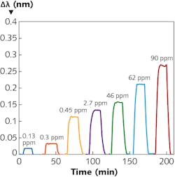
The SiN waveguide thickness is 300 nm, which works well for light in the 700–900 nm spectral range. One interferometric arm of the unbalanced Mach-Zehnder-based design is subjected to the gas under test, which is absorbed by the porous silica top cladding, slightly changing the effective refractive index of the arm through evanescent coupling. The time needed for enough absorption for a measurement is on the order of a few minutes. The light source for the device is a supercontinuum laser; detection is done using a broadband spectral analyzer made by Agilent (Santa Clara, CA). The figure shows response curves to acetone vapors at different concentrations from 130 ppb to 90 ppm. Although the experimental device has no way of distinguishing between different gases, future versions will have more-advanced mesoporous coatings that can selectively adsorb specific gases, and possible multiple interferometers on a single chip to sense different sorts of gases. Reference: G. Antonacci et al., APL Photonics, 5, 081301 (2020); https://doi.org/10.1063/5.0013577.

John Wallace | Senior Technical Editor (1998-2022)
John Wallace was with Laser Focus World for nearly 25 years, retiring in late June 2022. He obtained a bachelor's degree in mechanical engineering and physics at Rutgers University and a master's in optical engineering at the University of Rochester. Before becoming an editor, John worked as an engineer at RCA, Exxon, Eastman Kodak, and GCA Corporation.