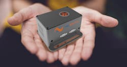
Si-Ware Systems unveils palm-sized mid-IR spectral sensing platform
Fabless semiconductor company Si-Ware Systems (Los Angeles, CA) has introduced what it says is the first highly compact mid-infrared (MIR) spectral sensing platform that offers wide wavelength coverage; the device is intended for detection and quantification of chemical compounds for quality control and quality assurance. The company's NeoSpectra-MIR platform includes off-the-shelf and custom application-specific products for solid, liquid, and gas detection.
The platform fits in the palm of one's hand, is lower in cost than benchtop equipment, can be used on-site as a test station or installed directly onto a pipe or into a production line, and eliminates the time and work required to send samples out to a central lab for testing, says Si-Ware. Other advantages listed by the company include robustness to shock/vibration, low maintenance, wide wavelength coverage that enables measuring multiple target chemicals (such as gases), and the ability to add target chemicals as requirements change.
Si-Ware Systems notes that it has developed a series of product demonstrators that can be used off-the-shelf, and that customized models can be configured and optimized with a toolkit. The modular components include the optical core module, the electronics, sampling interfaces, software and connectivity tools, chemometrics, and system-level packaging. The core technology could even be incorporated into a handheld or drone mounted devices, according to Si-Ware.
"There is strong demand for cost-effective, capable spectral sensing systems across many sectors," said Bassam Saadany, CTO/COO and founder of Si-Ware Systems. "The NeoSpectra-MIR Platform offers the size, flexibility and accuracy required for those who need complex spectral sensing on-site or on the production floor."
At the heart of the platform is a sensor based on Fourier-transform infrared (FT-IR) technology, a standard technique that offers a wide spectral range for qualification and quantification of materials. The sensors use patented microelectromechanical systems (MEMS) technology that enable a Michelson interferometer to be created monolithically on a MEMS chip.
The NeoSpectra-MIR platform is the latest addition to the NeoSpectra spectral sensing family, following on the heels of the NIR NeoSpectra-Scanner, a portable and handheld device, and the NeoSpectra-Micro sensor. Si-Ware Systems says it has shipped thousands of NeoSpectra product family units.
NeoSpectra's Yasser Sabry will be presenting a livestream presentation on the NeoSpectra-MIR platform's capabilities at SciX 2020 at 2 pm Eastern on October 15.
Source: Si-Ware Systems
About the Author
John Wallace
Senior Technical Editor (1998-2022)
John Wallace was with Laser Focus World for nearly 25 years, retiring in late June 2022. He obtained a bachelor's degree in mechanical engineering and physics at Rutgers University and a master's in optical engineering at the University of Rochester. Before becoming an editor, John worked as an engineer at RCA, Exxon, Eastman Kodak, and GCA Corporation.

