Frequency-domain terahertz systems poised for miniaturization
Terahertz radiation is a very useful tool. In contrast to x-rays, terahertz radiation is non-ionizing yet many materials, which are opaque to our eyes, are transparent in the terahertz region of the electromagnetic spectrum. An obvious and widely discussed application of this effect has been airport security. However, in the end, millimeter-wave scanners won the race for body scanning.
While in its infancy, terahertz scanning applications have great potential for industrial measurements, such as measuring the exact thickness of thin dielectric layers. Today, terahertz scanners measure the thickness of paint layers in the automotive industry, the thickness of foils in packaging, or check tablets inside opaque blisters. New devices based on telecom technology and frequency-domain spectroscopy make the technology faster, and thus create interest in more fields of application such as imaging sensors.
Industrial applications need simple and, most often, portable solutions. For example, radar developed for defense applications decreased in system size significantly over time as opportunities increased. Currently, radar’s optical analog lidar is shrinking systems down to chip-size, solid-state devices, driven by autonomous vehicle application requirements.
Terahertz technology is following a similar path. It must be smaller, faster, and cheaper; moving parts must be eliminated; and it appears lessons learned from radar and lidar may aid terahertz technology development.
Up to now, generating and detecting terahertz radiation has been a major bottleneck for more widespread use. Systems such as gyrotrons or synchrotrons are too big. Other solutions need complex optical systems with sensitive moving elements. The problem has been under discussion for 40 years, and so far, most solutions were not suitable for industrial applications.
In the last two decades, the invention of compact femtosecond fiber lasers stimulated the development of fiber-coupled, pulsed terahertz systems relying on ultrafast photoswitches. Their benefits for the measurement of various materials including polymers, paint and coatings, pharmaceuticals, electronics, petrochemicals, gases, and paper and wood have been discussed in the scientific literature.1 In these systems, a femtosecond laser pulse is used to generate an ultrashort current in a light-sensitive, biased semiconductor. This allows for the generation of broadband terahertz pulses with a bandwidth of more than 6 THz.
As the terahertz detection uses the reverse process, an additional copy of the original ultrashort laser pulse is required. Hence, the method relies on complex laser systems and moving optical elements for the necessary time delay of the two femtosecond pulses (see Fig. 1). Nevertheless, the method enables multilayer thickness measurements with a resolution of a few microns.A compact source based on telecom components
A new terahertz system, which has been developed by scientists at Fraunhofer Heinrich Hertz Institute (Berlin, Germany), relies on simple continuous-wave (CW) lasers instead of complex femtosecond pulsed sources. It uses two off-the-shelf telecom lasers, one with a fixed-frequency and a second sweeping laser source. The latter is a modulated-grating Y-branch laser, which uses the Vernier effect with two multipeak reflectors to achieve wide-frequency tuning over the whole telecom c-band from 1530 to 1565 nm. Mixed with the fixed-frequency laser, a spectral range from about 0.1 to more than 3 THz can be covered without any moving components.
Figure 2 shows a schematic of the system architecture and the measurement setup. It starts with the fixed-frequency or static laser, and the swept laser. Both laser signals are superimposed in a fiber coupler and amplified in a standard erbium-doped fiber amplifier (EDFA). The mixed signal carries the beat (or difference) frequency of the two input signals. This optical beat note is converted into terahertz radiation by a photodiode originally developed for and commercially used in high-speed fiber optical communication links. The emitted terahertz signal is guided from the emitter to the receiver with a pair of parabolic mirrors. The receiver mixes the incoming terahertz signal and the beat note of the second optical arm down to an intermediate frequency.The measured signal is amplified (transimpedance amplifier TIA) and digitized by the data acquisition unit (DAQ) together with the sample and cycling trigger of the sweep laser. This way, the setup can record a wide terahertz spectrum by simply sweeping the frequency of one of the two input lasers. The spectrometer is connected to a PC via USB. This system is fully fiber-coupled and does not contain any moving parts. The only free-space optics are in the contact-free sensor head. More details on the setup and measurement can be found in the scientific literature.2
It should be mentioned that the system relies on the concept of optoelectronic frequency-modulated continuous-wave (FMCW) terahertz spectroscopy. While popular with radar, this technique has been applied for the first time to terahertz spectroscopy. It uses the swept and delayed laser signal in a self-heterodyning scheme for phase-sensitive detection. Based on this method, the amplitude and phase of the terahertz signal can be recovered with software-based lock-in detection. In contrast to previous concepts, this scheme does not require any phase modulator. Therefore, it simplifies the architecture, increases the speed, and eliminates additional noise sources from the CW terahertz spectrometer. Details on the FMCW spectrometer were recently published in Nature Communications.3
Frequency vs. time-domain measurements
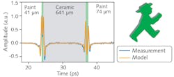
The most obvious terahertz thickness measurement can be made in the time domain (TDS). A sub-picosecond terahertz pulse is sent to the test surface and a sequence of peaks in the reflected signal provides the thickness information (see Fig. 3). This is a typical approach for measurements based on ultrashort (femtosecond to picosecond) laser pulses. Figure 1 shows the actual setup, which requires a laser pulse for both terahertz generation and detection; note that the curve is recorded point by point using a variable optical delay line and correlation techniques. Obviously, this requires the precise movement of several components for every measurement.Terahertz measurements based on frequency-domain spectroscopy (FDS) record the phase and the amplitude of the reflected spectrum. The time-domain signal is calculated by Fourier transformation and the layer thickness can be reconstructed from the data analogously to the time-of-flight approach shown in Figure 3. The resolution of the system is determined by two parameters: The frequency resolution of the spectrometer and its bandwidth. The higher the bandwidth, the better the temporal resolution and thus, the accuracy of the thickness measurement.
Reaching sub-micron precision with terahertz FDS measurements
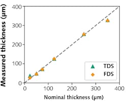
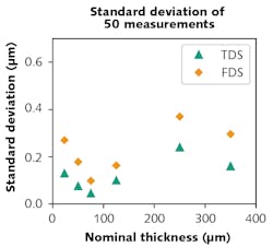
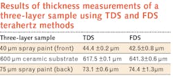
For a direct comparison of TDS and FDS methods, a setup using the same measurement head was employed and just the terahertz source was exchanged. In these experiments, single-layer Kapton foils with thicknesses between 50 and 75 µm, as well as PET foils with 23–350 µm, were used. The results (see Fig. 4) confirm that both methods can determine the foil thickness within the technical limits.Towards 3D terahertz measurements
The system used in these measurements was assembled from discrete components. As we know from telecom applications, all of these components and thereby the whole system can be realized in integrated optics as well. Such a miniaturization would not only reduce the size of the system by more than a factor of 10, it would also allow to scale up the production of the measurement system remarkably.
This path of miniaturization and integration of the new FDS terahertz measurement system is subject of the ongoing project TeraWay (ict-teraway.eu) funded by the European Union. It targets the full integration of both laser sources plus the amplifier on a single photonic integrated circuit (PIC). Reducing the whole system to chip size could enable automated production and significant cost savings. It would also allow for parallelization in, for example, imaging applications. This would have the prospect of 3D measurements since all optical phase information is recorded, which again would be analog to previous achievements in radar and lidar technology.
REFERENCES
1. M. Naftaly, N. Vieweg, and A. Deninger, Sensors, 19, 4203 (2019); https://doi.org/10.3390/s19194203.
2. L. Liebermeister et al., J. Infrared Millim. Terahertz Waves, 40, 288–296 (2019); https://doi.org/10.1007/s10762-018-0563-6.
3. L. Liebermeister et al., Nat. Commun. (2021); https://doi.org/10.1038/s41467-021-21260-x.

Andreas Thoss | Contributing Editor, Germany
Andreas Thoss is the Managing Director of THOSS Media (Berlin) and has many years of experience in photonics-related research, publishing, marketing, and public relations. He worked with John Wiley & Sons until 2010, when he founded THOSS Media. In 2012, he founded the scientific journal Advanced Optical Technologies. His university research focused on ultrashort and ultra-intense laser pulses, and he holds several patents.
Björn Globisch | Head, Terahertz Sensor Systems Group at the Fraunhofer Institute for Telecommunications
Björn Globisch is Professor for Physics at the Technical University Berlin and head of the Terahertz Sensors and Systems research group at the Fraunhofer Institute for Telecommunications (Fraunhofer HHI; Berlin, Germany).
Lars Liebermeister | Project Manager and Principal Scientist for terahertz system development, Fraunhofer Institute for Telecommunications
Lars Liebermeister is project manager and principal scientist for terahertz system development at the Fraunhofer Institute for Telecommunications (Fraunhofer HHI; Berlin, Germany).
