Photonic sensor technology inches towards consumer applications
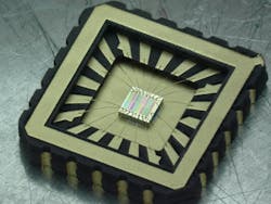
Spectral sensor technology company MantiSpectra (Eindhoven, Netherlands) has won the Hermes Award at Hannover Messe in Germany for ChipSense—a spectral sensor on a chip (see figure). Backed by photonics ecosystem creator PhotonDelta, MantiSpectra is using integrated photonics to significantly reduce the size and cost of material sensors.
By reducing the associated costs and adding efficiency and portability, the company hopes to enable opens more automation and innovation. To date, the technology has enjoyed quick adoption within a range of industries—it is now being used by three of the top 10 global beverage companies, several Fortune 500 companies, and is now entering trials with the Dutch National Police.
We recently connected with MantiSpectra managing director Maurangelo Petruzzella to learn more.
Laser Focus World: Can you briefly describe how ChipSense works?
Maurangelo Petruzzella: MantiSpectra has developed spectral sensors in the near-infrared (near-IR) range capable of classifying and quantifying material composition. Our core technology ChipSense is based on high-performance detectors having selective wavelengths in the near-IR region (850–1700 nm). This photonic chip provides a discrete near-IR fingerprint of the material under analysis. When combining this near-IR fingerprint with AI, the system can be trained for classification and quantification.
The ChipSense technology is a result of research at the Eindhoven University of Technology. There is a revolutionary change of perspective in thinking about spectroscopy. We went from building a miniaturized spectrometer to a spectral sensor on a chip.
It was great to prove that the first design, based on a double membrane structure, enabled the first miniaturized spectrometer, which traditionally are big systems that can only be operated by professionals. Though it had a nice resolution with narrow linewidths, it had a limited operating range, and it was rather hard to use outside the lab due to the presence of a movable mechanical part. We realized that we needed to change the approach: the wavelength range needed to be increased and we need to make it fit for a chip. We ended up with a rather simple structure without any moving elements. The spectral chip contains an array of resonant-cavity enhanced photodetectors, each featuring a distinct spectral response in the 850–1700 nm wavelength range, with a high signal-to-noise ratio. This high signal-to-noise ratio is key for high prediction accuracies in actual applications.
LFW: What do you see as the most exciting application opportunities?
Petruzzella: We are currently focusing on the agri-food sector. In food and beverage, ChipSense has already been employed by three of the top-10 food and beverage companies in the world and multiple Fortune F500 companies. The main problem is today, quality control is inefficient and the main cause of product recall. Food companies need to constantly send samples to external laboratories for quality control. This procedure takes a few days to weeks, with an average cost of 50 to 100 dollars per analysis. Plus, quality control is typically carried out only at the end of the process. ChipSense offers an immediate solution to measure material properties instantly, in seconds instead of weeks, in multiple steps of food production: at incoming raw material, during the process for real-time analysis, and after the production before shipping the final products.
LFW: How do you see ChipSense continuing to evolve?
Petruzzella: We are currently working on co-integrating electronics and photonics on the same platform, to achieve a form factor and price that will unlock the full potential of spectroscopy for volume markets. When scaling up the volumes, the costs of the sensor will reduce further. Imagine all the applications possible with our miniaturized near-IR device that can fit into a smartphone camera. This will drive a new revolution, like the silent revolution of having GPS in our smartphones. Getting access to the information of the world surrounding us will become as simple as getting the directions from going to A to B in a city.
While our current technology is used mainly in industrial applications, it will follow the same evolution of GPS or an inertial sensor, from research labs to high-value industrial applications, to the consumer. The key is the photonic integration and the fact that it is a semiconductor technology. We produce thousands of chips on just one wafer! This is the reason why we call it the Spectral Revolution!

Peter Fretty | Market Leader, Digital Infrastructure
Peter Fretty began his role as the Market Leader, Digital Infrastructure in September 2024. He also serves as Group Editorial Director for Laser Focus World and Vision Systems Design, and previously served as Editor in Chief of Laser Focus World from October 2021 to June 2023. Prior to that, he was Technology Editor for IndustryWeek for two years.
As a highly experienced journalist, he has regularly covered advances in manufacturing, information technology, and software. He has written thousands of feature articles, cover stories, and white papers for an assortment of trade journals, business publications, and consumer magazines.
