Photonics research at the Massachusetts Institute of Technology (MIT; Cambridge, MA) has taken many directions; it is the task of the university’s Center for Integrated Photonic Systems (CIPS) to draw them together to form a cohesive, institute-wide research community. At the CIPS Annual Meeting 2006 (May 4-5) held at MIT, Rajeev Ram, director of CIPS, noted in his opening statement that the organization also aims to participate in working groups of companies and researchers in defining the future of photonics.
Ram outlined some of the capabilities in photonics that exist at MIT, using the advent of a photonic-crystal illuminator as an example. As a doctoral student at MIT, Alexei Erchak developed a gallium arsenide-based light-emitting diode (LED) with a photonic-crystal structure that boosted light output. The device was designed and tested, manufacturing techniques were researched, and economic analysis was done; Erchak went on to found Luminus Devices (Woburn, MA), where he is currently the chief technical officer. The company produces the PhlatLight, a photonic-crystal LED powerful enough to illuminate high-definition TVs.
Plenary talks at CIPS 2006 included one by Michael Lebby of the Optoelectronics Industry development Association (Washington, D.C.) on worldwide market trends in optoelectronic technologies; one on naval electro-optics by Tom Giallorenzi of the Naval Research Laboratory (Washington, D.C.); and a third by Alan Wilner, president of the IEEE Lasers and Electro-optics Society (Piscataway, NJ) on integrated photonics for smart communications systems, in which he encouraged the development of photonic “plug-and-play” devices (difficult as that may be), as well as optical networks that can monitor and manage themselves.
Sessions run the gamut
Technical sessions included several with an emphasis on the communications aspect of photonics, including optical broadband, all-optical networking, photonics for quantum information processing (QIP), electronic and photonic integrated circuits, and high-speed interconnects. Other sessions moved into far-ranging areas such as advanced displays, next-generation solar cells, and biophotonics.
Karl Berggren of MIT introduced the QIP session by noting that a sort of Moore’s Law can be applied to factoring large numbers (important in cracking complex codes), in which factoring improves by about five decimal digits a year. Practical quantum computing would extend this trend. Quantum cryptography, however, would make codes secure against this threat.
In the first QIP talk, Alexei Trifonov, chief scientist and vice president of MagiQ (New York, NY), described the company’s product for quantum-key distribution, which guarantees secure communication over a 100 km distance in optical fiber using the transmission of single photons. Jeffrey Shapiro, director of MIT’s Research Laboratory of Electronics, then spoke about some work he and Franco Wong of MIT are engaged in to develop-using photonic quantum gates-an eavesdropping attack on quantum-key distribution. Their attack only hopes to extract the maximum possible information from the channel; that is, to make the key-distribution system’s job as challenging as possible (the fundamental security of the system would not be compromised).
Sae-Woo Nam of the National Institute of Standards and Technology (NIST; Boulder, CO) summed up NIST’s work on single-photon sources and detectors, explaining the critical distinction between photon-counting detectors, which can detect individual photons but can’t resolve differences between pulses containing one, two, or three photons, and photon-number-resolving detectors, which can accomplish this task. He also described an efficient entangled-photon source being developed at NIST.
Isaac Chuang of MIT described the challenges inherent in detecting single ions and controlling their locations in a planar ion trap. The result is a “dance” where individual clouds of ions can be marched across a sample surface at will. Ultimately, this trapping system will have to be integrated with an enormous array of controlled optical beams of UV light and photodetectors.
The biophotonics session was introduced by Ram, who noted that the term “biophotonics” has become generic, encompassing things like ordinary optical microscopes; he proposed that the term be defined as “innovation in photonics driven by biology, biotechnology, and medicine.” Mehmet Yanik of MIT, in the first talk, centered on the use of femtosecond laser pulses to perform nanosurgery on individual neurons, enabling the study of nerve regeneration. He is currently developing new tools to allow surgery at the tens-of-nanometers scale to enable characterization of synaptic junctions.
Tom Jeys of the MIT Lincoln Laboratories (Lexington, MA) presented requirements for optical bioaerosol sensors, demonstrating that multicolor fluorescence spectroscopy on aerosol particles could discriminate spores from background particles (which has been integrated into a system ready for field use). He discussed his recent work trying to lower the cost of these sensors by moving to UV LED excitation.
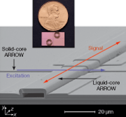
Holger Schmidt of the University of California at Santa Barbara presented his silicon-based platform for guiding light within a waveguide containing a liquid core, used for sampling fluids via fluorescence down to the 100-femtoliter scale and making possible single-molecule detection in a planar, integrated platform (see figure). He discussed preliminary results on sensing individual ribosomes with the waveguides.
Harry Lee of MIT discussed recent work at MIT on a microscale bioreactor to facilitate the development of industrial bioprocesses. The microfluidic platform uses integrated fluorescence sensors to stabilize the growth environment of bacteria to enable reproducible development of new biomaterials such as vaccines, polymers, and pharmaceuticals.

