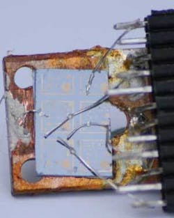
Stimulated emission and the resulting coherent amplification arising from many roundtrips of a beam in a resonant cavity are what make a laser different from a light bulb (and a maser different from common microwave sources). Researchers at the University of Nottingham (Nottingham, England) and the V. E. Lashkarev Institute of Semiconductor Physics (Kiev, Ukraine) have created an acoustic version, called a “saser” (sound amplification by stimulated emission of radiation) that emits a beam of phonons.1
The structure of the device, which includes a gallium arsenide/aluminum arsenide (GaAs/AlAs) semiconductor superlattice, is surprisingly similar to that of a distributed-feedback optical laser. “The superlattice is the gain medium of the saser structure, in which electron population inversion for phonon emission is achieved by passing an electrical current,” says Anthony Kent, one of the researchers. “However, the superlattice also acts to confine the phonons, so it acts like a distributed-feedback cavity. It is not the fact that the materials are semiconducting that is important from the point of view of phonon confinement; it is that the two semiconductor materials that make up the superlattice have different densities and speeds of sound. This means they have different acoustic impedances, and so sound is reflected at the interfaces between GaAs and AlAs. This is very similar to an optical Bragg mirror, where it is the different refractive indices that give rise to optical reflection.”
A 50-period superlattice was grown on a semi-insulating GaAs substrate with one 5.9-mm-thick GaAs well and one 3.9-mm-thick AlAs barrier per period, and electrical contacts were formed with the emitter and collector layers. The “miniband” width of the superlattice was 0.7 meV. The device was electrically pumped, with a threshold of 75 mV, and was cryogenically cooled to 2 K.
Using a superconducting bolometer to detect the phonon radiation, the researchers took measurements at 0° and 30° from the axis of the device, discovering a clear peak at 2.1 meV at 0° and no peak at 30°. This resonance corresponds to the point at which the electrical-energy drop per superlattice period equals the energy of the first superlattice mini-Brillouin zone-center phonon mode; in other words, it is evidence for saser action (the researchers meticulously looked at other possible causes of the peak, such as a directional peak in emissivity at that energy for the superlattice, and discounted them). The 2.1 mV phonon energy corresponds to a sound frequency of 510 GHz—a frequency far higher than what any conventional ultrasound device emits.
The measured phonon-emission power (on the order of milliwatts per square centimeter) was less than theory predicted; the researchers have taken this as a good sign, believing that there is room to improve the output power. Uses could include the acoustic analog of optical spectroscopy, as well as the imaging of nanostructures.
REFERENCE
1. A.J. Kent et al., Phys. Rev. Lett. 96, 215504 (June 2, 2006).
About the Author
John Wallace
Senior Technical Editor (1998-2022)
John Wallace was with Laser Focus World for nearly 25 years, retiring in late June 2022. He obtained a bachelor's degree in mechanical engineering and physics at Rutgers University and a master's in optical engineering at the University of Rochester. Before becoming an editor, John worked as an engineer at RCA, Exxon, Eastman Kodak, and GCA Corporation.
