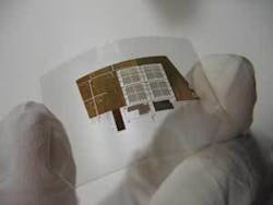
Flexible silicon expands application possibilities
Single-crystal semiconductor materials such as silicon (Si) and gallium arsenide have previously been transferred to flexible polymers to create thin-film transistors (TFTs) on plastic; however, the process is limited and cumbersome. Researchers at the University of Wisconsin-Madison (Madison, WI) have instead developed a simpler, more versatile transfer technique that allows them to create strained-silicon TFTs with high drive current and high transconductance, making them excellent candidates for use in displays, solar cells, and biosystem implants.
The TFT active layer is formed as a thin membrane on silicon-on-insulator (SOI) substrates. Both strained- and unstrained-silicon TFTs are fabricated in a similar process using a sandwich structure of Si and silicon-germanium alloy. Photolithography is used to pattern the membrane, which is then transferred (using a “dry” printing method) to a flexible polyethylene substrate onto which a layer of photoresist has been applied that serves as both an adhesive and as the gate-dielectric layer for the TFTs. Contact Zhenqiang Ma at [email protected].

