QUANTUM-DOT SOURCES: Quantum-dot development pursues new applications
Despite the initial expectations of high differential gain, the modulation response of quantum-dot (QD) lasers has remained limited in the most interesting 1300- to 1550-nm wavelength region. New applications, however, do take advantage of unique features of quantum dots.
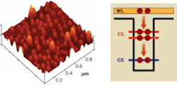
Quantum dots are semiconductor nanostructures in which electrons and holes are confined into nanometer-size islands of a low-bandgap semiconductor like indium arsenide (InAs) within a higher-bandgap matrix, such as gallium arsenide (GaAs) or indium phosphide (InP). Because of the three-dimensional (3-D) confinement, the energy levels in each island are discrete, much like in atoms (see Fig. 1, right), in contrast to the continuous dispersion relations of bulk and quantum-well (QW) active materials. This characteristic raised hopes that the QD gain spectrum would be narrower, and the peak gain and differential gain higher, for a perfectly uniform array of QDs.1
While rather uniform QD arrays have been realized by growth on nanopatterned substrates, room-temperature lasing has been achieved only by using planar, self-assembled epitaxial growth techniques.2, 3 Deposition of InAs in appropriate conditions, for instance, results in the spontaneous formation of flat In(Ga)As islands on top of a 2-D In(Ga)As “wetting” layer or WL (see Fig. 1, left). This growth mode is favored over conventional 2-D growth since partial relaxation of the compressive strain can occur on top of the InAs islands, lowering the elastic energy. A higher local indium concentration, and thus a longer emission wavelength, is possible in QDs, as compared to QWs.
Gain spectrum
The energy spectrum of a single QD is discrete, but the dispersion in QD sizes resulting from the spontaneous nucleation process produces a dispersion of energy levels, and consequent inhomogeneous broadening of several tens of nanometers in the gain spectrum. The gain spectrum of self-assembled QDs is thus broader, and the peak gain lower as compared to conventional QWs. The gain value is further limited by the maximum surface density of QDs.
For QDs the material gain is not a well-defined parameter because its use implies that the gain would scale with the QD volume, which is not correct as long as the optical wave interacts with a single quantum state. Modal gain is a more adequate measure of gain. Typical maximum values (for 1300‑nm QDs) in a typical edge-emitting laser structure fall more than 10 times lower than the maximum modal gain achievable with QWs (a difference that is easily ascribed to the lower density of states and the larger spectral width). A low modal gain requires low cavity loss and severely impacts the laser modulation response through gain saturation, as observed in first generations of QD lasers.
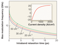
When the gain of the lowest energy state in the band (“ground state,” GS) is too low, the device tends to lase on upper energy levels (“excited states,” ES), which have higher degeneracy and thus higher gain. A strong effort has thus been dedicated to improving the modal gain by stacking several layers of QDs. This task is nontrivial, as the strain produced by the lower layers changes the growth conditions of upper layers. Much progress has been achieved recently, particularly by NL Nanosemiconductor (Dortmund, Germany), with state-of-the-art modal gain values in the 20- to 30-cm-1 range in ten-layer QD laser structures (see Fig. 2, inset).4 These values allow GS lasing in as-cleaved edge-emitting devices as short as 600 µm, and prevent gain saturation, resulting in modulation rates up to 10 Gbit/s.4,5Modulation properties
The possibility of modulating a laser at a given frequency depends on the coupling between carriers and photons-as measured by the differential gain-and ultimately by the damping introduced by any slow time constants in the system as measured by the gain compression factor. The intraband relaxation time (that is, the time it takes an injected electron to relax down to the GS) affects both the differential gain (by producing an accumulation of carriers on higher-energy states) and the gain compression factor (through hole burning), and can ultimately limit the modulation bandwidth. Intraband relaxation rates are slower in QDs than in QWs (intraband carrier relaxation consists of the sequence of carrier capture from the WL into the QD and a stepwise cascade through the various energy levels) because the energy differences do not in general match the optical phonon energy. Relaxation proceeds through higher-order processes such as multiphonon or carrier-carrier scattering.
The combined capture and interlevel relaxation process from the WL to the GS of an empty QD typically takes several picoseconds, as determined by time-resolved photoluminescence spectroscopy. Moreover, GS filling reduces the relaxation rate through Pauli blocking, particularly in a laser operating close to gain saturation. A detailed analysis shows that interlevel relaxation between the lowest ES and the GS is the limiting process for the modulation bandwidth. In particular, the maximum 3-dB modulation frequency can be approximately related to the relaxation time and the maximum modal gain (see Fig. 2).6 The modulation bandwidth can be increased by either increasing the available gain (the number of QDs) or reducing the relaxation time.
State-of-the-art 1300-nm QD lasers operate with relaxation times in the 3- to 6-ps range and modal gains of 20 to 30 cm-1, corresponding to a bandwidth close to 10 GHz.4, 5, 7 Similar bandwidths have been measured on InAs/InP QDs emitting at 1550 nm, while a much higher bandwidth of 22 GHz has been reported for InAs/GaAs QD lasers at 1100 nm, because of higher gain and shorter relaxation time obtained by a tunnel-injection structure.8 As the potential for large improvements in modal gain appears limited, bypassing the relaxation bottleneck by tunnel-injection schemes or by engineering the interlevel relaxation process will be needed for increasing the modulation bandwidth of 1300- to 1550-nm lasers.
Quantum-dot advantages
Despite their limited gain and modulation frequency, QD active regions have several advantages connected to their discrete density of states. First, the temperature dependence of the laser threshold current (measured by the characteristic temperature T0) can be much better than QW lasers because the electronic levels in the conduction band are spaced by more than the Boltzmann energy, kT, and thus little change in the population distribution occurs around room temperature. Temperature-independent operation between 20°C and 85°C has been achieved recently in 1300-nm lasers with p-doped QDs.
The idea behind p-doping the QDs is that hole levels are more closely spaced because of the larger effective mass, so that thermal spreading can occur in the valence band: by forcing a large hole population the quasi-Fermi level is pushed deep in the band and a constant hole occupation of the lasing state is ensured.9 Experimentally, p-doping increases the room-temperature threshold-current density (due to increased nonradiative recombination and optical loss), but also makes it temperature-independent up to 85°C, eliminating the need for active cooling and temperature control.
A second advantage of QD lasers is the possibility of engineering the linewidth-enhancement factor (LEF) or gain-phase coupling. Indeed, because of the Gaussian distribution of QD sizes, a symmetric gain spectrum is obtained from the GS, resulting in very low (less than 1) LEF and low chirp, as demonstrated experimentally.7 On the other hand, if the laser is operated close to GS gain saturation, the differential gain becomes very small and asymmetric, leading to very large values of the LEF (greater than 50 has been reported), and opening the way to pure phase modulation in a QD amplifier.10 These characteristics are intimately connected to the discrete density of states of the QD active region.
Finally, the large inhomogeneous broadening can be turned into an advantage for applications that require a broad gain spectrum, such as tunable lasers, semiconductor optical amplifiers (SOAs), and superluminescent diodes (SLEDs). Quantum-dot SOAs and SLEDs also have the potential for a large saturation output power, due to the presence of a carrier reservoir in the ES and WL.
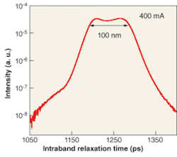
Quantum-dot SOAs with 20-dB chip gain over a 120-nm bandwidth around 1500 nm have been demonstrated, although the strong polarization dependence is still preventing applications as in-line amplifiers.11 In contrast, polarization dependence is not an issue for QD SLEDs, which can be used as sources for optical coherence tomography in both the 1050- and the 1300-nm wavelength regions, of interest for medical applications.By using chirped QD multilayers and combining GS and ES gain spectra, a spectral width as large as 120 nm has been achieved (see Fig. 3).12 Further optimization is under way to achieve a more Gaussian-shaped spectral linewidth (and thus reduce the coherence length), and further increase the output power (currently in the 1- to 10-mW range).
While QDs have not fulfilled the old dream of an atomic-like gain material, their quantized energy spectrum brings several other advantages, including temperature insensitivity, small chirp, and broad gain spectrum, making them appealing for several industrial applications. A European consortium (FP6 integrated project “ZODIAC”) comprising several industrial and academic laboratories, is currently investigating the application of QD active regions in directly modulated lasers, tunable lasers, and amplifiers.13 Superluminescent LED applications are being investigated by SLED vendor Exalos (Zurich, Switzerland).
REFERENCES
1. Y. Arakawa, H. Sakaki, Appl. Phys. Lett. 40, 939 (1982).
2. M.H. Baier, S. Watanabe, E. Pelucchi, E. Kapon, Appl. Phys. Lett. 84, 1943 (2004).
3. D. Bimberg, M. Grundmann, N.N. Ledentsov, Quantum Dot Heterostructures, John Wiley & Sons (Chichester 1999).
4. K. Otsubo et al., Japanese J. Appl. Physics Part 2-Lett. & Express Lett. 43, L1124 (2004).
5. M. Kuntz et al., Elect. Lett. 41, 244 (2005).
6. M. Sugawara et al., J. Phys. D Appl. Phys. 38, 2126 (2005).
7. Z. Mi, P. Bhattacharya, S. Fathpour, Appl. Phys. Lett. 86, 153109 (2005).
8. S. Ghosh, S. Pradhan, and P. Bhattacharya, Appl. Phys. Lett. 81, 3055 (2002).
9. O.B. Shchekin and D.G. Deppe, Appl. Phys. Lett. 80, 3277 (2002).
10. B. Dagens et al., Elect. Lett. 41, 323 (2005).
11. T. Akiyama et al., IEEE Photonic Tech. Lett. 17, 1614 (2005).
12. L.H. Li et al., Elect. Lett. 41, 41 (2005).
13. www.if.pwr.wroc.pl/zodiac.
Andrea Fiore | Group Leader, EPFL Institute of Photonics and Quantum Electronics
Andrea Fiore is group leader at Ecole Polytechnique Fédérale de Lausanne (EPFL)’s Institute of Photonics and Quantum Electronics (Lausanne, Switzerland).
Alexander Markus | Postdoctoral Scientist, EPFL Institute of Photonics and Quantum Electronics
Alexander Markus is a postdoctoral scientist at Ecole Polytechnique Fédérale de Lausanne (EPFL)’s Institute of Photonics and Quantum Electronics (Lausanne, Switzerland).
Lianhe H. Li | Postdoctoral Scientist, EPFL Institute of Photonics and Quantum Electronics
Lianhe H. Li is a postdoctoral scientist at Ecole Polytechnique Fédérale de Lausanne (EPFL)’s Institute of Photonics and Quantum Electronics (Lausanne, Switzerland).
Marco Rossetti | R&D Manager, Exalos AG
Marco Rossetti, Ph.D., is R&D manager at Exalos AG (Schlieren, Switzerland), and was a graduate student at Ecole Polytechnique Fédérale de Lausanne (EPFL)’s Institute of Photonics and Quantum Electronics (Lausanne, Switzerland).


