Nanophotonic Imaging: Nanoantenna captures plasmon-spectrum images
Conventional optical microscopy is based on the detection of photons emitted from an object. But scientists at the Swiss Federal Institute of Technology (ETH; Zurich, Switzerland), The Zuse Institute Berlin (Berlin, Germany), and the University of Potsdam (Potsdam, Germany) are able to image an object without the need to illuminate it or communicate with it directly in any way.1 Instead, the researchers scan a single gold nanoparticle acting as a nanoantenna through the near field of a sample and image that sample by studying how the intrinsic radiative properties of the gold nanoparticle are modified, which they do by monitoring the particle’s plasmon spectrum.
Based on experiments using a single gold nanoparticle as a subwavelength antenna with oscillating dipoles, recent developments in nano-optics show that the linewidth and transition frequency of a dipole respond sensitively to the optical contrast of its nanoscopic environment; in effect, the spectral modifications of a nanoantenna can serve as the signal for a novel mode of scanning near-field optical microscopy (SNOM). The size, shape, and refractive index of a metallic particle, as well as the optical constants of its surroundings, all influence the collective excitation of free electrons that can give rise to plasmon resonances.
For spherical particles in a homogeneous medium, the plasmon spectrum can be calculated using Mie theory based on a so-called multipole expansion. In gold nanoparticles 100 nm in diameter or smaller, optical response is predominantly due to the dipolar mode of the plasmon excitation. Their ability to be detected even down to a size of 5 nm, as well as their large quantum yield and photostability, make gold nanoparticles excellent dipolar antenna with well-defined resonance frequency and linewidth.
In the imaging experiment, the scientists send white light from a xenon lamp through a 100-µm-core-diameter multimode fiber and then through a polarizer. A lens system weakly focuses the light onto a gold nanoparticle mounted on the end of an uncoated glass-fiber tip. Scattered light from the nanoparticle is collected by a microscope objective attached to another multimode fiber and sent to a spectrometer fitted with a cooled CCD camera.
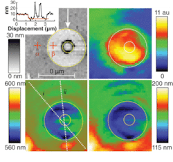
The scientists fabricated an imaging sample consisting of approximately 2‑µm-diameter round openings in a semitransparent chromium film on a cover glass with very sharp edges rising up less than 10 nm. The sample was placed on an SNOM stage on a 3-D piezoelectric scanner and positioned to within 5 to 10 nm of the gold nanoparticle using shear-force feedback. In addition to a shear-force topography image of the sample, the plasmon spectrum of the gold nanoparticle was recorded by triggering the spectrometer camera at each of the 1600 pixels of the 40 × 40-pixel scan (see figure).
Measuring spectral changes
To analyze the plasmon resonance from the nanoparticle in the vicinity of the sample, the scientists applied a phenomenological model to quantify the observed spectral modification, based on the definition of an effective polarizability for a metallic nanoparticle. The model allows the scientists to determine very small changes in the peak positions of the FWHM (full width at half maximum) of the spectra, translating into an image of the circular glass openings in the chromium film.
The spatial resolution of this method-an edge sharpness observed to be 170 to 370 nm-depends on the size of the nanoantenna. Experiments using very small gold nanoparticles may push the resolution of their method further toward the nanometer level.
“The fascinating part of our approach is that we can detect very small changes of the intrinsic resonance properties of the nanoantenna,” says researcher Vahid Sandoghdar. “There is a certain intellectual challenge to have so much control over the nanoworld to be able to measure such things. It would be particularly exciting to shrink the size of the nanoantenna to a single molecule. At that point, one would measure energy level shifts of a quantum emitter due to its near-field interaction with its nanoenvironment—in the extreme case, another single molecule.”
REFERENCE
1. T. Kalkbrenner et al., Physical Rev. Lett.95, 200801 (2005).

Gail Overton | Senior Editor (2004-2020)
Gail has more than 30 years of engineering, marketing, product management, and editorial experience in the photonics and optical communications industry. Before joining the staff at Laser Focus World in 2004, she held many product management and product marketing roles in the fiber-optics industry, most notably at Hughes (El Segundo, CA), GTE Labs (Waltham, MA), Corning (Corning, NY), Photon Kinetics (Beaverton, OR), and Newport Corporation (Irvine, CA). During her marketing career, Gail published articles in WDM Solutions and Sensors magazine and traveled internationally to conduct product and sales training. Gail received her BS degree in physics, with an emphasis in optics, from San Diego State University in San Diego, CA in May 1986.
