OPTOELECTRONIC INTEGRATION: Hybrid laser combines III-V gain with silicon waveguide
Researchers at the University of California Santa Barbara (UCSB) have bonded nonsilicon semiconductor optical-gain layers directly to a silicon laser cavity to fabricate a hybrid alternative to silicon Raman lasers that is an order of magnitude shorter. The optically pumped evanescent 1538-nm laser operates in pulsed mode, has a lasing threshold of 30-mW average power, puts out 1.4 mW of average power, and represents a first step toward an electrically pumped hybrid silicon laser (the device has also been operated in continuous wave).
Developed by John Bowers, professor of electrical and computer engineering at UCSB, and his students, Alex Fang and Hyundai Park, the laser uses indium aluminum gallium arsenide (InAlGaAs) quantum wells to provide optical amplification. Their wafer-scale fabrication approach allows the optical waveguide to be defined by CMOS-compatible silicon processing, while optical gain is provided by III-V materials. The quantum-well structure is bonded to the silicon wafer using low-temperature oxygen-plasma-assisted wafer bonding.1
“The ability to combine the best of both worlds (III-V gain material with silicon photonics) could lead to a new way of enabling highly integrated laser sources with intelligent optoelectronic devices for future optical communications at low cost,” Bowers said.
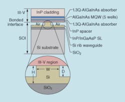
The actual device was divided into two regions, a silicon-on-insulator (SOI) passive-waveguide structure and a III-V optically active region. The SOI structure consisted of a silicon substrate, a 500-nm-thick silica lower cladding layer, and a silicon rib waveguide with a height (H), width (W) and rib-etch depth (D) of 0.97, 1.3, and 0.78 µm, respectively. The III-V region consisted of an indium phosphide (InP)-indium gallium arsenic phosphide (InGaAsP) superlattice, an InP spacer, five InAlGaAs quantum wells sandwiched between two AlGaInAs separated confinement heterostructure (SCH) layers, and an InP upper cladding layer.
The device structure can be extended directly from optical to electrical pumping by including doped layers and patterning mesa structures in III-V regions to flow electrical currents through the III-V active region, according to the researchers. Bowers added that the method should also prove useful for building other optically active devices, including amplifiers, modulators, and detectors.
REFERENCE
1. H. Park, A.W. Fang, S. Kodama, J.E. Bowers, Optics Express13(23) 9460 (Nov. 14, 2005).
Hassaun A. Jones-Bey | Senior Editor and Freelance Writer
Hassaun A. Jones-Bey was a senior editor and then freelance writer for Laser Focus World.
