Super-resolution Microscopy: Approach boosts accuracy of single-molecule tracking

Tracking how molecules move, form shapes, and interact within neurons and other cells offers a powerful view of biological processes that impact health. Now, work at Stanford University (CA), led by Nobel Laureate W. E. Moerner, demonstrates a marked improvement in the accuracy of such tracking—and of super-resolution microscopy in general.1
A single point of light coming from a molecule can typically be located with ~10 nm precision. At such resolutions, any imperfection in an optical system introduces image distortions that can significantly skew measurements, particularly in 3D. The resulting errors could mean the difference between interpreting two molecules as interacting or simply residing nearby.
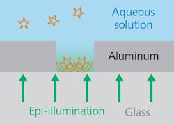
Such aberrations have not generally been recognized, says doctoral candidate Alex von Diezmann, but his team demonstrated their existence—and their ability to degrade images. Seeking a better calibration approach, von Diezmann created an array of holes in a metal film, each smaller than 200 nm and regularly spaced 2.5 μm apart. Once the holes were filled with fluorescent dyes, he was able to use the array to adjust for optical errors across the microscope's entire field of view (not just at a few select spots, as is possible using current methods).
Studying the new calibration technique with double-helix and astigmatic point spread functions, the researchers found aberrations resulting in 20% measurement errors in 3D, and corrected them. In addition, they have used the technique to reduce aberrations of 50–100 nm to just 25 nm.
The team notes that aberration correction will become increasingly important as optical microscopy techniques evolve, and says the new approach can be used with any super-resolution or localization microscopy requiring 3D precision.
1. A. von Diezmann, M. Y. Lee, M. D. Lew, and W. E. Moerner, Optica, 2, 11, 985–993 (2015); doi:10.1364/optica.2.000985.

Barbara Gefvert | Editor-in-Chief, BioOptics World (2008-2020)
Barbara G. Gefvert has been a science and technology editor and writer since 1987, and served as editor in chief on multiple publications, including Sensors magazine for nearly a decade.