NANOSCALE IMAGING: Nanometer-resolution imager uses a 13 nm tabletop source
Nanoscale imaging techniques such as scanning electron microscopy, superresolution multiphoton microscopy, stimulated emission-depletion microscopy, and coherent anti-Stokes Raman scattering microscopy cannot image samples greater than 100 nm thick and have relatively poor contrast, require fluorescent labeling, or are label-free but have only modest resolution gains compared to traditional confocal microscopy, respectively. Consequently, scientists and engineers are constantly working to improve these nanometer-regime imaging technologies.
Soft x-ray coherent diffractive imaging (XCDI) has emerged as a complementary nanoscale technique that can provide high spatial resolution, elemental and chemical specificity, and even image thick samples in two and three dimensions. However, synchrotrons and x-ray free-electron lasers (XFELs) used as imaging sources are only available in a few research laboratories due to high cost and complexity.
The recent availability of tabletop X-ray sources has enabled capture of nanoscale images at resolution values of 30–50 nm, albeit with integration times as long as 80 min. But researchers from JILA at the University of Colorado–Boulder, the SLAC National Accelerator Laboratory (Menlo Park, CA), the University of California–Berkeley, Colorado State University (Fort Collins, CO), and UCLA are dramatically changing the XCDI picture by using a 13 nm tabletop x-ray source to achieve 25 nm resolution imaging in only 30 s.1
High-harmonic generation
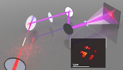
In XCDI imaging, an object is illuminated with a coherent plane wavefront with a relatively narrow spectral bandwidth, scattered light is recorded by a CCD, and an iterative phase-retrieval algorithm reconstructs an image from a scattered-light diffraction pattern. The illumination source is produced by focusing a 780 nm ultrafast Ti:sapphire laser-amplifier system with 2 mJ pulse energy, 2 kHz repetition rate, and 25 fs pulse duration into a 5-cm-long, 150-μm-diameter, helium-filled hollow waveguide, resulting in a coherent, laserlike high-harmonic 13 nm output beam. Zirconium filters are used to reject the driving-laser light that propagates along with the desired 13 nm output, and a hybrid input-output (HIO) phase-retrieval algorithm is used to reconstruct the specimen from the CCD diffraction pattern (see figure).
Using the XCDI imaging system, scattered-light diffraction patterns were recorded 3.6 cm from the sample, corresponding to a numerical aperture (NA) of ~0.36. Using a knife-edge criterion, a resolution of 25 nm was measured in reconstructed images of chevron-style patterns obtained from 30-s exposures. The imaging technique is scalable; imaging speeds and resolution to sub-10-nm levels could be achieved by increasing photon flux and decreasing illumination wavelength.
Beyond 2D imaging, ankylography or tomography algorithms can be used to create 3D images. With 0.6 NA and using the same chevron-style objects fabricated on a 50- to 100-nm-thick silicon nitride membrane, 3D experimental reconstructions were obtained using ankylography.
“This technique has the potential to produce images with ultrahigh resolution in three dimensions with better than 10 fs temporal resolution,” says postdoctoral researcher Daniel Adams at JILA. “Further development of this tool will have a real impact on nanoscience and with the advantage of its compactness, will be an important tool for university-scale research centers.”
REFERENCE
1. M.D. Seaberg et al., scheduled for November 2011 nonlinear optics focus issue, Opt. Exp.

Gail Overton | Senior Editor (2004-2020)
Gail has more than 30 years of engineering, marketing, product management, and editorial experience in the photonics and optical communications industry. Before joining the staff at Laser Focus World in 2004, she held many product management and product marketing roles in the fiber-optics industry, most notably at Hughes (El Segundo, CA), GTE Labs (Waltham, MA), Corning (Corning, NY), Photon Kinetics (Beaverton, OR), and Newport Corporation (Irvine, CA). During her marketing career, Gail published articles in WDM Solutions and Sensors magazine and traveled internationally to conduct product and sales training. Gail received her BS degree in physics, with an emphasis in optics, from San Diego State University in San Diego, CA in May 1986.
