Quantum-dot PC laser has lowest-threshold emission
For applications such as on-chip and intrachip optical communications, electrically pumped lasers with compact size, low power dissipation, and low-threshold operation are needed. Unfortunately, photonic-crystal (PC) nanocavity and microcavity lasers only offer ultralow nanowatt-range thresholds through optical pumping, because electrically pumped devices have proven challenging to fabricate. But researchers at Stanford University (Stanford, CA), Lawrence Berkeley National Laboratory (Berkeley, CA), and the University of California–Berkeley have succeeded in developing an electrically pumped, quantum-dot-based PC laser with a threshold-power dissipation of only 181 nA at 50 K—comparable to optically pumped PC lasers, and 1000 times smaller than the best conventional vertical-cavity surface-emitting lasers (VCSELs).
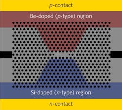
The team achieved this record threshold by developing a simple, flexible fabrication procedure that gives better control of current flow through the laser’s tiny cavity. A lateral p-i-n region is created in a PC lattice composed of a beryllium-doped p-type region, a silicon-doped n-type region, and a three-hole-defect gain region incorporating three layers of high-density indium arsenide (InAs) quantum dots. In this configuration, current flow is defined lithographically to flow only to the active region of the diode, making the device very efficient.
Contact Jelena Vuckovic at [email protected].

Gail Overton | Senior Editor (2004-2020)
Gail has more than 30 years of engineering, marketing, product management, and editorial experience in the photonics and optical communications industry. Before joining the staff at Laser Focus World in 2004, she held many product management and product marketing roles in the fiber-optics industry, most notably at Hughes (El Segundo, CA), GTE Labs (Waltham, MA), Corning (Corning, NY), Photon Kinetics (Beaverton, OR), and Newport Corporation (Irvine, CA). During her marketing career, Gail published articles in WDM Solutions and Sensors magazine and traveled internationally to conduct product and sales training. Gail received her BS degree in physics, with an emphasis in optics, from San Diego State University in San Diego, CA in May 1986.
