Robert L. Gunshor and Arto V. Nurmikko
Compound semiconductors such as gallium arsenide and related III-V materials typically emit within the infrared spectral region. Devices based on these materials are useful in applications such as optical-fiber communication links and compact-disk players. Wide-bandgap II-VI compound semiconductors, however, can have a range of direct energy gaps that allow emission over the complete range of the visible spectrum with potentially good efficiency. Consequently, direct-bandgap II-VI semiconductor devices offer the most promise to access the green and blue portion of the visible spectrum.
The driving force behind research efforts into II-VI materials is the number of applications envisioned for short-wavelength laser-diode devices, such as in medical diagnostics and bright displays. Application to high-density optical data storage, however, may be more significant because the reduction of wavelength by a factor of two can increase the data-storage area density by a factor of four.
Both fundamental and practical problems dealing with material quality in II-VI systems have created major obstacles to their early implementation. As a result, by the late 1970s the II-VI semiconductors were largely relegated to academic research among a small community of workers. In the early 1980s, research efforts were initiated primarily in the USA and Japan to apply nonequilibrium epitaxial growth methods, such as molecular-beam epitaxy (MBE), to the growth of II-VI heterostructure semiconductors.
Initially, the development of epitaxial growth techniques was motivated by the potential to provide quantum-sized heterostructures (such as implemented in III-V compounds) and to avoid traditional defect and doping problems that had been associated with more conventional equilibrium-growth techniques used for growing bulk crystals. By the end of the decade, substantial progress had been made on II-VI multilayer structures (such as quantum wells and superlattices), and potentially useful heterostructures for light-emitting applications had been identified. Important advances also occurred in controlling the purity and defect generation in materials.
The development of techniques for p-type doping using nitrogen combined with accumulating knowledge of the physics of II-VI heterostructures and materials advances associated with MBE set the stage for prototype injection-laser devices. In 1991, a group at 3M Corporate Research Laboratories (St. Paul, MN) followed by our Brown University-Purdue University team announced the demonstration of such laser diodes, operated under pulsed excitation at cryogenic temperatures.1,2
Although the devices are currently confined to research laboratories, progress over the past three years has been substantial. The first demonstrations of room-temperature continuous-wave (CW) operation of the laser diodes were made roughly one year ago, with device lifetime before failure continuing to increase from seconds to about one hour.3,4
Device structure
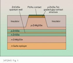
Most blue-green laser-diode devices are grown on GaAs substrates with a GaAs buffer layer upon which the II-VI compounds are grown using MBE. The structures have ZnMgSSe quaternary optical-cladding layers (a compound first used by Sony, Tokyo, Japan) with ZnSSe waveguiding regions and typically one to three ZnCdSe quantum wells that provide optical gain (see Fig. 1). The composition of the ZnSSe is chosen to provide a lattice match to GaAs, while the magnesium and sulfur fractions are adjusted to allow the bandgap to be varied and maintain lattice matching to GaAs. The quantum well is under compressive strain.
Current room-temperature CW devices emitting around 508 nm use a Zn(Se,Te) graded contact on the p-ZnSe layer.5 Earlier construction schemes had a contact to the p layer that was typically evaporated gold. Because of the insufficiently large work function of gold, a rectifying Schottky barrier provides the current injection. With evaporated gold contacts, the laser devices failed due to burning at poor contacts. The graded contact is currently the contact of choice for laser diodes, although a mercury-based contact for II-VI LED devices has also been developed at North Carolina State University (Raleigh, NC) by Jan Schetzina and coworkers.
The specific contact resistivity of the graded contact (about 4 × 10⁻⁴ Wcm-2) is currently about an order of magnitude higher than desired; thus, the contact raises the diode voltage needed. Once the limitations to device lifetime are resolved, the contact may become the limiting factor in determining device lifetime. Clearly, the contacts must be improved—possibly by modest modifications to the grading scheme or by a totally new concept. At the present time, room-temperature CW threshold currents as low as 250 A/cm2 with threshold voltages on the order of 5 V have been obtained.
We usually make index-guided devices with reactively etched mesas typically 4 µm wide. Devices are made with flip-chip heat-sinking, and SiO2/TiO2 multilayers are used for reflective facet coatings. Typically, room-temperature CW output powers are a few milliwatts, but pulsed operation provides power of several hundred milliwatts.
Recently, audiences have viewed "live demonstrations" of blue-green laser diodes used in our laser pointers at conference presentations. Because the sensitivity of the eye peaks in the green, the impression is that the blue-green laser beam is more intense than conventional red laser-beam pointers. Vertical-cavity surface-emitting laser operation has also been demonstrated using optical pumping techniques in heterostructures containing three ZnCdSe quantum wells.
Challenges
The most interesting challenges confronting technologists for device improvement are how to increase device lifetime and how to decrease the operating wavelength. Device lifetime is currently limited primarily by microstructural defects that produce nonradiative recombination in the gain portion of the laser. This effect reduces the gain of the active region until stimulated emission ceases. As of November 1994, the longest lifetime for a II-VI device operating CW at room temperature was one hour.6 Degradation evidently originates at crystalline defects, primarily stacking faults, that do not appear to be intrinsic to the growth/fabrication process.
A major focus of current research involves improving growth procedures to eliminate defects and the degradation processes similar to those that originally held back commercialization of GaAs-based laser diodes. The density of defects limiting device lifetime is about 1 × 10⁵ to 1 × 106 cm-2, about the same as in early GaAs-based devices with short lifetimes.
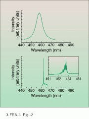
Extending device operation to shorter wavelengths is also under development. Room-temperature pulsed laser-diode operation at about 482 nm has been reported (see Laser Focus World, May 1994, p. 15). Recently, we made 460-nm devices (see Fig. 2).7 By comparison, the GaN-based blue LED also has a peak emission at 460 nm but with a spectral width of approximately 100 nm. The shorter-wavelength laser devices have not yet reached CW operation at room temperature, apparently due to an increased vertical impedance in the wider-bandgap materials.The electrical problem is seen in the increased threshold voltage for lasing (about 10 V for 460-nm devices). The difficulty originates in the rapid rise in the nitrogen-acceptor-activation energy observed as the bandgap of a p-type layer increases. Apparently, the dopant activation energy and resistivity increase as the bandgap increases, and the local lattice relaxation about the acceptor results in a deep energy level.8 Although this behavior occurs in some n-type dopants (DX centers), such behavior has not been previously observed in connection with acceptors in a p-type semiconductor. To overcome these effects, heterostructures exploiting "bandstructure engineering" ideas are being investigated.
It is clear that further efforts in material science, device physics, and engineering are needed before compact visible light sources such as room-temperature CW blue-green laser diodes reach the marketplace. Understanding and controlling the electrical properties of wide-bandgap II-VI multilayer structures is needed. The contact resistance and operating voltage need to be lowered, possibly by optimizing the formation of the GaAs/ZnSe heterovalent junction.
Simple evaporated gold contacts to p-ZnSe fail because of contact heating. Graded Zn(Se,Te) contacts have extended device lifetimes that are determined by the formation of regions of dark-line defects within the active layers of the devices, similar to a mechanism occurring in AlGaAs laser diodes. Defects such as stacking faults, threading dislocations, and point defects appear to cause degradation. Current efforts are directed at minimizing as-grown microstructural defects, as well as process-induced defects.
The motivation to improve the performance and lifetimes of this type of blue-green-emitting device is impelled by applications. A reliable CW blue diode laser at 400 nm would increase the information density stored and read on compact disks by nearly an order of magnitude.
REFERENCES
1. M. Haase, J. Qiu, J. DePuydt, and H. Cheng, Appl. Phys. Lett. 59, 1272 (Sept. 1991).
2. H. Jeon et al., Appl. Phys. Lett. 59, 3619 (Dec. 1991).
3. N. Nakayama et al., Electron. Lett. 29, 1488 (Aug. 1993).
4. Salokatve et al., Electron. Lett. 29, 2192 (Dec. 1993).
5. Y. Fan et al., Appl. Phys. Lett. 61, 3160 (Dec. 1992).
6. S. Itoh and A. Ishibashi, Proc. SPIE Conference on II-VI Blue/Green Laser Diodes, R. L. Gunshor and A. V. Nurmikko, eds., SPIE (1994).
7. D. C. Grillo et al., Electron. Lett. 30(25), 2131 (Dec. 1994).
8. J. Han et al., Appl. Phys. Lett. 65 (Dec. 1994).

