Microarrays are playing a critical role in genomic, proteomic, and drug-discovery research. Scientists are now integrating the illumination and detection processes on single chips for point-of-care diagnostics.
Since their introduction nearly 20 years ago, optical biochips-or microarrays-have generally been defined as very small sample substrates made of glass, plastic, or silicon that permit the simultaneous execution and evaluation of hundreds or even thousands of biochemical reactions. When used in conjunction with fluorophors (marker dyes) and laser-based scanners (typically 532 or 633 nm), commercial platforms such as the GeneChip from Affymetrix (Santa Clara, CA)-which is etched with microfluidic channels using manufacturing methods adapted from the semiconductor industry-or the cDNA/cRNA microarray from Agilent (Palo Alto, CA)- which is printed with molecular probes using inkjet technology originally developed at Hewlett Packard-are able to decode individual genes, identify disease-specific proteins, and enhance the development of protein-based biodrugs.
Even in the early days, when the scanners were primarily large argon-ion lasers that took up an entire laboratory workbench, the combination of these technologies transformed biological research. Experiments that once took weeks, months, or even years to perform could now be completed in hours, providing new insights into conditions ranging from diabetes and cystic fibrosis to asthma and heart disease. In the 1990s the field was further enhanced by the introduction of frequency-doubled Nd:YAG lasers, which cut the size of most laser scanners in half, made the technology more affordable, and broadened the user base. In addition to academic research, pharmaceutical companies are now able to speed the development of new drugs based on more-accurate diagnoses and better understanding of biological mechanisms; it has been estimated that DNA and protein biochips have lowered average drug-screening costs from $2 to $0.0001 per test.1 In addition, given the current focus on bioterrorism, many manufacturers are working to create chips that can detect potentially harmful bioagents in the air, public water sources, and even our food.
Further technology innovations are likely to create even more opportunities for biochips, particularly in the diagnostic arena where fields such as systems biology are in their infancy but generating great excitement among researchers who believe that micro- and nanotechnologies will lead to a whole new way of treating disease: preventing it before it even occurs by understanding the molecular processes that cause it.2 Thus, like their counterparts in the semiconductor industry, biochip manufacturers are focused on further reducing the feature sizes on each chip to increase the number of samples that can be processed at one time. On the scanner side, next-generation solid-state blue lasers such as the directly doubled external-cavity Cyan laser from Picarro (Sunnyvale, CA) are drawing interest from bioinstrument companies because of their extremely low noise and their ability to access a wider range of fluorophors and fluorescence detection than 532-nm lasers.
All in one
Some researchers even envision the day when optical biochips and the analytical processes they enable can be further streamlined, combined in a single integrated chip that eliminates the need for separate scanning equipment. Not just a chip etched with hundreds of microfluidic channels or dotted with thousands of DNA or RNA probes, but one containing all of the illumination and detection components that identify various genes and proteins and tracks the process changes that occur within a cell when it is diseased or is exposed to a certain drug.
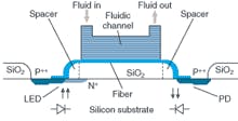
For example, the European BIOMIC (bioanalytical system based on an optical biochip) project, which concluded in 2004, yielded a bioanalytical lab on a chip based on a monolithic silicon optoelectronic transducer that can simultaneously measure eight different proteins or DNA fragments (see Fig. 1). Research teams in Greece, Denmark, and Italy joined forces with the Fraunhofer Institute for Biomedical Engineering (IBMT; St. Ingbert, Germany) on this project; the resulting multianalyte biochip is expected to be ready for market in the next few years.3
“For the most part we’re analyzing proteins or genetic material fragments,” said Hans-Heinrich Ruf, head of the biosensoric microsystems group at IBMT. “This makes the biochip ideally suited for various areas of biochemical analysis. The main targets are process monitoring in the pharmaceutical and food industries, for example, and for monitoring ecologically relevant materials.”
The real-time affinity biosensor combines an optocoupler, an LED light source (639 nm), an integrated silicon nitride optical fiber, and a photodetector to create a monolithic silicon optoelectronic transducer and a microfluidic module. According to Ruf, planar integrated waveguides show much potential for multianalyte testing and assay sensitivity because planar geometry facilitates multiple analyte arrays to be created via a number of methods, including ink-jet and contact printing, photolithographic patterning, photochemical attachment, and microfluidic network patterning. In addition, planar integrated waveguides could detect binding events in real time using evanescent field optics. The group is now working to improve the chip’s sensitivity.
“The improvements we intend are to increase the quantum efficiency of the LED,” he said. “A simple LED is not very effective at emitting light, so there is a lot of noise. But there are some tricks you can do with the LED to align the imaging junction directly under the entrance of the optical fiber and the end of the fiber to the junction of the photodiode.”
Multiple minilasers
Another EU-sponsored project, the Optical Biochip Consortium (www.cardiff.ac.uk/medicine/pathology/ research/optical_biochip_project.htm), is focused on reducing to microscale the light-emitting and collecting components currently used to analyze biological samples in a lab. The consortium is working to fabricate a laser-based lab on a chip integrated with “microtrafficking” systems to move samples and live cells around for processing. The goal is to use light to excite specially designed fluorescent chemicals that can reveal important features about each cell.
“As a medical microbiologist and cancer researcher, I have been involved for several years in working to advance imaging technologies, particularly to track real events in real time, which typically requires a lab full of equipment to allow you to look at specific events in cells,” said Paul Smith, professor of pathology at the University of Wales College of Medicine and head of the consortium. “But there is a new realization that testing at the cellular level can provide an enormous amount of information, and our concept is that miniaturization will allow this (at the point of care). Putting living cells on a chip is one way to do this.”
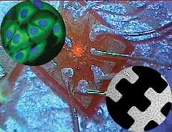
At the heart of the consortium’s approach is a gallium arsenide wafer that contains microelectronics, optoelectronics, and fluidic systems (see Fig. 2). The microfluidics are designed to move and manipulate cells, allowing them to be interrogated by various light beams that interact with fluorescent molecules used to tag various aspects of the cells. The resulting signals are captured using a macroscopic off-chip camera or on the chip itself. The goal is to develop and integrate an array of red-light-emitting devices, each the size of a single cell, that coincide with new fluorescent tags. The consortium plans to include multiple lasers of different wavelengths that can be switched on and off as needed. However, the primary aim is to implement two-photon excitation and optical traps to hold single cells at the focus of the laser beam to allow measurements or planned destruction of the light-sensitive tags. “It is likely that the functional chips will focus on specific applications in which not all functions are required by using discrete components, each optimized for a different function,” Smith said.
FIGURE 2. A montage shows human cells (top left) labeled with a green fluorescent protein and the live cell-penetrating far-red nuclear dye DRAQ5 (marked blue), a red-emitting laser chip array (center) and cells growing in microchannels (bottom right). OPTICAL BIOCHIP CONSORTIUM
So far, one year into the four-year project, the consortium has yielded a prototype chip, according to Smith. Other achievements include use of an excimer laser to sculpt features on a surface that are important for anchoring cells on that surface; development of a new series of dyes that can enter cells rapidly, emit in the far-IR, and be excited by red light; and fabricating chip arrays of up to eight lasers, each 10 µm in size (the size of a red blood cell).
The next step, said Smith, is the detection scheme. To channel and guide available light toward the detectors, and to sort them into different wavelengths (corresponding to the different tags), the chips will include microfabricated lenses and mirrors.
“We are particularly interested in looking at the fluorescence signature on the probes and the fluorescence lifetime, which we think is important for diagnostics. And not just using dyes, but infrared dyes,” he said. “But our project is not just to produce a product. We think in terms of products to give us a target, such as drug discovery, but what we are trying to do is bring together the issues of solving the technology of an optical computer, an optical chip, that can interface with life.”
Better detection
A group from Stanford University (Palo Alto, CA) has been focusing on integrated detection systems for lab-on-a-chip applications, particularly for detecting fluorescence at longer IR wavelengths.4 As part of his Ph.D. dissertation, Evan Thrush and colleagues developed a monolithically integrated semiconductor sensor for fluorescence detection on a microfluidic platform (see Fig. 3). According to Thrush, they combined 773-nm vertical-cavity surface-emitting lasers, p-i-n photodetectors, and optical-emission filters on a single gallium arsenide (GaAs) substrate. The components are optically coupled to a glass microfluidic channel through the use of a discrete microlens to form a complete sensor with theoretical detection sensitivity of 40 nanomolar, compared to 10 to 100 picomolar for conventional lab equipment. But Thrush believes that this sensor is capable of subnanomolar sensitivity by using a different material for the filter.
“People have wanted to integrate detection systems for lab-on-a-chip applications with particular interest in fluorescence because it is such a widely used detection methodology,” said Thrush, who is now at Agilent. “What differentiates our research is that this is the first to truly capitalize on semiconductor technologies, which offer great advantages for making devices more cost effectively. We think there will be huge gains in cost reductions and highly parallel architectures.”
Thrush sees this sensor more for hand-held diagnostic applications than as something that would compete with, say, Affymetrix or Agilent microarray scanners in the laboratory. He believes that the integration of microfluidic systems with chemical processing and analysis will enable miniaturized total-analysis systems for point-of-care applications and enable the detection of common diseases, pathogens, and early-stage cancer.
“A lot of people have not liked our technology because we use more unconventional markers that work in the near- or deep-IR,” he said. “But if you talk about diagnostic settings where you want to analyze more-complex biologic fluids, moving into the longer wavelengths is very important because you get less background fluorescence.”
REFERENCES
- Technical Insights (Frost & Sullivan) (May 13, 2004).
- Science 306, 5696 (Oct. 22, 2004).
- K. Misiakos, S. E. Kakabakos, P. S. Petrou, and H. H. Ruf, Analytical Chemistry 76(5) (March 1, 2004).
- E. Thrush et al., Sensors and Actuators, in press.
Kathy Kincade
contributing editor


