A two-photon 3-D lithography technique that uses light-activated molecules to selectively initiate chemical reactions within polymers and other materials could provide an efficient way to produce complex structures with submicron features. Organic dye molecules known as Bis-donor phenylene vinylenes can absorb two photons simultaneously. When excited, the molecules transfer an electron to form a simple acid or a radical group that can initiate a chemical reaction such as polymer cross-linking or ion reduction.
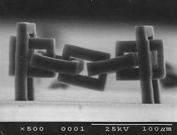
A microchain structure fabricated with a 3-D two-photon lithographic process is an example of a structure that would be difficult to produce layer-by-layer with 2-D lithographic processes. The microchain links are topologically connected, but not directly anchored to the surface.
By adding small concentrations (0.1%) of the molecules to a resin slab containing crosslinkable acrylate monomer, for example, researchers can use a focused near-IR laser beam to draw patterns and initiate crosslinking reactions exclusively in material exposed to the light, according to Seth Marder, a researcher at the Georgia Institute of Technology (Atlanta, GA) who described the technique earlier this year at the annual meeting of the American Association for the Advancement of Science (AAAS). The reactions can make that portion of the slab insoluble, allowing the remainder to be washed away to leave a complex 3-D structure.
The molecules developed by Marder and collaborator Joseph Perry are a couple orders of magnitude more efficient at absorbing two photons than previously available photoactive materials. That efficiency allows them to write 3-D patterns in polymer slabs that are typically 100 µm thick at light intensities low enough to avoid damaging the materials (see figure). And they have demonstrated the ability to create both positive and negative resists using two-photon activated reactions to alternatively create soluble or insoluble 3-D patterns.
Beyond polymers, the researchers have also fabricated tiny silver wires from patterns written in materials containing silver nanoparticles and ions. The process may eventually compete with existing processes for fabricating microfluidic devices, photonic-bandgap structures, optical-storage devices, photonic switches and couplers, sensors, actuators, micromachines—and even scaffolds for growing living tissue.
The laser-writing process takes advantage of the fact that the chemical reaction occurs only where molecules have absorbed two photons. Since the rate of two-photon absorption drops off rapidly with distance from the laser's focal point, only molecules at the focal point receive enough light to absorb two photons. "We can define with a very high degree of precision in the x, y, and z coordinates where we are getting excitation," Marder explained. "Using 700-nm light, the patterning precision can be about 200 nm across by 800 nm in depth."
