newsbreaks
Fractal zone plates produce fractal intensity distributions
A group at the Universidad Politécnica de Valencia (Valencia, Spain) has proposed a new kind of Fresnel zone plate that has a fractal zonal structure, which produces an axial focus distribution that has fractal qualities for monochromatic illumination. A fractal zone plate has, within each of its zones, smaller zones that imitate the larger zone pattern. The group has determined that the lacunarity, or relative gap widths, of the zones has a drastic effect on the axial intensity distribution, although the fractal nature of the distribution is always maintained. Certain null points appear at the same axial positions for any lacunarity; in between, the fine structure changes.
Although they currently qualify as esoterica, fractal zone plates could play a part in multifocal contact lenses for the correction of presbyopia, say the researchers. Before this happens, however, a mechanism to control the diffraction efficiency must be developed. Although the modeling was done for binary fractal zone plates, the researchers are investigating nonbinary versions, including the effects of optical aberrations and polychromatic illumination, as well as creating nonrotationally symmetric versions. Contact Walter Furan at [email protected].
Double tunneling barrier suppresses dark current in QDIP
For use with long-wave IR light, quantum-dot IR photodetectors (QDIPs) have a relatively high dark current resulting from thermionic emission and field-assisted tunneling. The existing techniques for reducing the dark current also reduce the desired photocurrent as well, forcing a compromise in the detector design. Researchers at the University of Michigan (Ann Arbor, MI) have developed a detector architecture based on double-barrier resonant tunneling that results in a large reduction in dark current for QDIPs.
The detector’s heterostructure contains two tunneling barriers that are spaced to cause a tunneling resonance that coincides with the photo-excited carrier energy. The resulting near-unity tunneling probability exists only for the photo-excited energy, resulting in suppression of dark current. The heterostructure is contained within each quantum-dot layer. An experimental tunneling-QDIP device was grown by molecular-beam epitaxy and compared to a conventional QDIP. The detectors had a 600-µm-diameter illuminated area. The tunneling architecture resulted in a reduction of the dark current by approximately two orders of magnitude over a range of bias voltages from 0 to 2.5 V. Contact Pallab Bhattacharya at [email protected].
Miniature atomic clock uses MEMS fabrication techniques
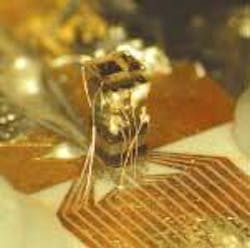
The smallest atomic-frequency references reported to date have a volume of 1 cm3 but dissipate several watts of electrical power. Unfortunately, high power consumption and poor frequency stability prohibit the use of these atomic-clock candidates for such portable applications as anti-jam global-positioning systems. But scientists at the National Institute of Standards and Technology (NIST; Boulder, CO) have significantly reduced the size and power consumption of the core physics assembly of an atomic clock through microelectromechanical-systems (MEMS) fabrication techniques.
The atomic-clock core is fabricated as a sandwich of several key layers: a vertical-cavity surface-emitting laser complete with micro-optics to produce collimated, attenuated, and polarized light; a cesium vapor cell; various optical neutral-density filter layers; and, finally, a silicon p-i-n photodiode. The operation of the frequency reference is based on coherent population trapping in which two optical fields generate a coherent “dark state” in the atomic hyperfine transition at their difference frequency. The clock has a power dissipation of only 75 mW and timing precision at the microsecond level over a 24-hour period. Contact Svenja Knappe at [email protected].
Tin oxide nanoribbons become optical waveguides
Chemists at the University of California-Berkeley and the Department of Energy’s Lawrence Berkeley National Laboratory (Berkeley, CA) have demonstrated that semiconductor nanoribbons can serve as optical waveguides, potentially for optoelectronic integrated circuits. The manipulation of light within submicrometer volumes could eventually lead to optical computers and a photonic internet with data-transmission speeds of 160 Gbit/s (thousands of times faster than today’s high-speed Internet connections).
The single-crystal nanoribbons were fabricated from tin oxide, a wide-bandgap (3.6-eV) semiconductor material that acts as an excellent waveguide for visible and UV light when the ribbon is 100 to 400 nm wide and thick. With lengths up to 1500 µm, the flexible ribbons can be repeatedly curved into loops with radii as small as 5 µm-unusual for a crystal that is brittle in bulk form. While the losses of 1 to 8 dB/mm were significantly higher than those reported for silica waveguides, the losses are far better than what is required for integrated planar photonic applications that only require light transmission over submicrometer distances. Contact Peidong Yang at [email protected].
Simple autocorrelator measures microscope pulse broadening
Ultrafast lasers provide the high peak intensities needed for multiphoton techniques in nonlinear optical microscopy. But the optics in the microscope itself can broaden the femtosecond pulses, reducing nonlinear excitation efficiency. Various techniques have been conceived for measuring the pulse-broadening caused by microscope optics. Researchers at the Istituto Nazionale di Ottica Applicata Largo E. Fermi (Firenze, Italy) have developed the simplest yet- a small wavefront-division lateral-shearing interferometer (LSI) that can be inserted directly into the instrument’s optical path, and is used in combination with a fluorescent uniform specimen.
A white-light-compensated LSI for use in collimated light consisted of two 6-mm-thick glass plates at an angle of 45°. The plates were cut from the same substrate to ensure virtually no path-length difference, and thus broadband operation. For the experiment, a commercial confocal-laser-scanning microscope was modified for nonlinear operation. A specimen with single-photon emission and absorption peaks of 458 and 516 nm, respectively, was used, and was excited into two-photon fluorescence by the microscope’s Ti:sapphire laser. In the shear direction, the fluorescence intensity profile was proportional to the second-order autocorrelation function, allowing the pulse width to be determined. Contact Franco Quercioli at [email protected].
Single-cell photonic-crystal laser is electrically driven
A single-cell, low-threshold-current, electrically driven photonic-crystal laser has been demonstrated by researchers from the physics department of the Korea Advanced Institute of Science and Technology and from the Electronics and Telecommunications Research Institute (both of Daejeon, Korea).
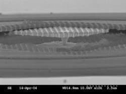
The main difficulty overcome by the researchers was figuring out how to make electrical contact with the photonic-crystal-resonator structure. Without degrading the quality factor of the mode, a central indium phosphide diamond-shaped post with a height of 1 µm and diagonal widths of 0.64a and 0.51a (a= 510 nm, the lattice constant of the crystal) was fabricated at the center of a single-cell photonic-crystal cavity. Holes were injected directly through the bottom of the post, while electrons were supplied laterally from the top electrode of the 282.5-nm-thick semiconductor-heterojunction n-i-p structure with its crystal lattice of different air-hole sizes. The photonic-crystal cavity was electrically pulse-pumped at room temperature and produced monopole-mode lasing at 1519.7 nm from its top surface. A low-threshold current of approximately 260 µA was measured; an excellent first step in the ultimate development of a thresholdless laser. Contact Yong-Hee Lee at [email protected].
Pure isotopic carbon senses pressure in diamond-anvil cell
Diamond-anvil pressure cells are built by polishing the tips of two diamonds and then applying force, producing high pressure in a sample placed between the polished surfaces. By illuminating the sample with laser light through the diamond, Raman spectroscopy and other optical techniques can be used to analyze the sample properties.
The use of a diamond anvil by itself for stress or pressure sensing is not suitable because the resulting Raman signal from the carbon (C) is a convolution of complicated stress states in the large sampling volume. Recent advances in microwave-plasma chemical-vapor-deposition processes have made it possible to grow thin layers of isotopically mixed or pure 12C or 13C that allow uniformity of the stress state over the smaller sampled region. A 20-µm homoepitaxial 13C layer grown over the flattened tip of a natural-abundance 12C diamond by researchers at the University of Alabama at Birmingham (Birmingham, AL) has an intense Raman signal that is not masked by the Raman signal from the natural diamond, allowing quasi-linear correlation of the observed Raman spectra within the diamond-anvil chamber to ultrahigh pressures in the range of 50 to 100 GPa. Contact Yogesh K. Vohra at [email protected].
SNOM photolithography produces 20-nm features
Fabricating sub-30-nm features on semiconductor chips via photolithography is normally considered the province of extreme-UV (EUV) lithography. While only a photomask-based approach like EUV can mass-produce chips, penlike writing approaches may be usable if a low output suitable for research is all that is required. For example, a near-field scanning optical microscope (NSOM) can write nanolines in photoresist; the NSOM technique is low-cost, functioning in air rather than the vacuum required for other writing techniques such as electron-beam and focused-ion-beam lithography.
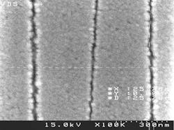
Scientists at the Data Storage Institute (Singapore) have now written lines as small as 20 nm in width using an NSOM. The light source, a frequency-doubled ultrafast laser emitting 100-fs pulses at a 400-nm wavelength, produces nonlinear effects in the resist, resulting in features much smaller than the NSOM’s 50-nm aperture width. Low laser power (below 0.01 mW) and writing speed (8 µm/s for the 20-nm features) results in smaller widths and shallower depths. The researchers believe that, with process and photoresist improvements, they can bring linewidths down to 5 nm. Contact Hong Minghui at [email protected].
Glass reversibly softens under very low-power laser light
Scientists at Ohio State University (Columbus, OH) have found that germanium-selenium (GexSe1−x) glass (which is used in the electronics industry) softens by nearly 50% when exposed to very low-level laser light and hardens back into its original condition when the light is switched off. The effect is reversible and is not thermally induced. The discovery was made by accident as the physicists were trying to study the properties of the material.
While probing the elasticity of the glass through Brillouin scattering (in which near-bandgap light at 647.1 nm was focused to a 50-µm spot in the glass), the scientists noted inconsistencies that related to the optical power of the laser probe itself. The effect occurred only when the Ge proportion x was at or near 0.19, which is the material’s so-called rigidity-transition point. At this point, the glass softened from a hardness of 26 to 13 GPa as the laser power increased from 2 to 6 mW. The glass rehardened completely when the laser light was blocked. The researchers hypothesize that the minimum-stress nature of the transition point may lead to changes in molecular bonds, causing the softening. Contact Ratnasingham Sooryakumar at [email protected].


