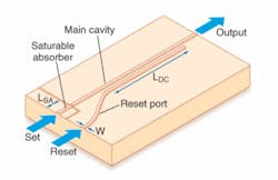
Scientists at the University of Tokyo (Tokyo, Japan) have demonstrated the first bistable laser diode in which both set and reset operations can be performed optically.1 The existing design could potentially operate at 2 GHz, a speed that could be improved upon in future iterations, say researchers Mitsuru Takenaka and Yoshiaki Nakano. Their hope is that the bistable laser diode will eventually be part of a set of all-optical devices that can replace electronics for those digital functions that must be performed in optical networking—each time a signal passes through an optical/electronic interface, both time and power are lost.
The bistable laser diode has been around for a long time, but it has always required an electronic pulse reset. Though various options have been considered to get around this problem, none have been successful until now. The new work has exploited an idea that has previously been used in all-optical switches and wavelength converters—the nonlinear directional coupler (NLDC). This is a waveguide placed very close to the laser diode that couples to it only when light is present. Thus, it has the advantage of being easily integrated and providing a second mechanism through which light can interact with the laser diode.
The saturable absorber prevents lasing from spontaneously occurring in the main cavity, despite the current flowing through it, by absorbing sufficient energy to keep it below threshold (see figure). When it is irradiated, however, its ability to absorb drops, thus allowing the laser to turn on. Even once the "set" light has been removed, emissions from the main cavity are able to keep the absorption low so that lasing can continue. Thus, once switched, the device is latched in the on position. Sending a "reset" signal then allows energy to be coupled out of the laser diode, preventing lasing and reasserting the quenching effect of the saturable absorber. The device is then latched off.
Fabrication of the bistable laser diode was straightforward, as the processes used were the same as other similar devices. The active layer was an indium gallium arsenide phosphide multiple-quantum-well structure deposited by metal-organic vaporphase epitaxy—the ridge waveguides were photolithographically defined and then selectively wet-etched. One innovation the team made, however, was to avoid masking steps by using a shadowing technique. To electrically isolate the two adjacent waveguides, they tilted the wafer to 75°, coating only one side of the structures with the titanium silver conducting material. The resulting isolation resistance was 4 kΩ.
The device already works (all that was required was careful setting of the currents controlling the two waveguides), but making the device smaller will likely solve some minor problems. One issue with the final device was that although the set beam could take a relatively wide range of wavelengths (1530 to 1575 nm), the reset was more restricted—it had to be within 10 nm of the design wavelength of the laser diode (1563 nm). This was because the bend in the waveguide structure was somewhat absorptive. By making it smaller, the range could be improved. Further, researchers say that by making the entire device shorter, they would reap the added benefits of improving the on/off contrast to 20 dB from 10 dB, and improving the switching speed, which is partly restricted by the resonant frequency.
REFERENCE
- M. Takenaka and Y. Nakano, IEEE Phot.Tech. Lett. 16(1) (January 2004).
About the Author
Sunny Bains
Contributing Editor
Sunny Bains is a contributing editor for Laser Focus World and a technical journalist based in London, England.
