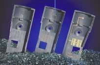
As mobile and other electronic devices become more sophisticated, the traditional two-dimensional (2-D) circuit board appears on the way to being replaced by controlling circuitry directly patterned on three-dimensional (3-D) device contours (see figure). A laser-based method of accomplishing this—laser-direct structuring (LDS) of 3-D molded interconnected devices (3D-MIDs)—essentially consists of optically writing circuit patterns directly from computer-aided-design (CAD) data onto an injection-molded, laser-sensitive plastic substrate and then adding the actual circuits through an electroless plating process.
Three steps of a laser-direct-structuring process begin with laser-sensitive injection-molded plastic (left). Laser scribing of a circuit design from CAD data is the second step (middle). An electroless-plating step deposits the actual circuit (right).
While it is possible to mold actual circuit boards, design flexibility is severely limited, according to Stephan Smith, general manager of LPKF Laser & Electronics North America (Wilsonville, OR), with international headquarters in Garbsen, Germany. "We wanted to come up with a product that doesn't have those stringent design restrictions and that is also more flexible and quicker to use," he said. The LDS 3D-MID process was actually developed in a multi-institutional collaboration between industry and academia initially funded by the German Science Ministry.
"We were part of the larger project for the laser portion, and since then we have taken the lead as far as finalizing the project, which includes responsibility for the plastic modification as well," he said. Last November, LPKF signed a license agreement with plastics manufacturer Ticona (Kelsterbach, Germany) to fabricate 3D-MID laser-sensitive substrates in a heat resistant liquid-crystal polymer that is intended to withstand the high temperatures required for lead-free solder connections in mobile communications devices, hearing aids, and sensory technology in automobiles.
The substrate consists of an injection-moldable plastic doped with a metal-based organic compound that undergoes a local physiochemical reaction upon laser activation, exposing metal atoms along the intended circuit path prior to deposition of the actual circuitry in the electroless plating step. The laser activation comes from a 1064-nm-emitting Nd:YVO4 (vanadate) laser operating at a pulse repetition rate between 1 and 100 kHz with a minimum beam diameter of 40 µm. Line widths as small as 150 µm with 200-µm spacing are written using a galvanometer scanner; height adjustments are made through an f-theta lens for an overall writing speed on the order of 4000 mm/s.
Numerous industrial and technological collaborations are involved in the process. As a laser manufacturer with a proprietary recipe for laser-activated plastics, LPKF must license the recipe to plastics manufacturers, which currently include Degussa (Düsseldorf, Germany) and Bayer (Leverkusen, Germany) in addition to Tikona. Also in November, at the Productronica trade fair in Munich, Germany, LPKF signed an agreement with the Harting Technology Group (Espelkamp, Germany) to provide LDS 3D-MID technology to create solderable micropackaging devices for semiconductors.
So far, a wide range of licensed materials has become available, from low-cost polypropylene to high-temperature-resistant liquid-crystal polymer. The real challenge, however, lies in merging processes from two separate industries—plastics and circuit boards. "The circuit-board people always had to follow a certain form to put a circuit board into a typically plastic housing, such as in a cell phone," he said. "More recently, flexible components have become available that follow housing shapes more aggressively but that are not part of the housing itself. That is something this technology will accomplish."
