PHOTONIC FRONTIERS: THIN-FILM PHOTOVOLTAICS: The key to success is higher efficiency

The rapidly growing solar-cell market is dominated by crystalline-silicon devices, thanks to advantages including light-conversion efficiency up to 20% in production units. However, the silicon wafer substrates used in the solar cells account for more than half of module manufacturing costs, and developers are concerned that existing silicon supplies won’t keep up with the demand for building large solar-photovoltaic energy farms.1 Those cost and supply issues are pushing interest in thin-film photovoltaics as the best way to reduce solar cell cost to $1 per watt of generating capacity.
Deposited on glass substrates or flexible metal sheets, thin-film solar cells require only micrometer-scale layers of expensive semiconductor materials. Already on the market are second-generation solar cells based on thin films such as amorphous silicon and cadmium telluride. Meanwhile, developers have ambitious plans for a third generation of solar cells that would match or beat the efficiency of crystalline silicon in converting sunlight to electricity.
It’s about time–in a world needing clean, green energy. But the challenges are serious.
Cost and performance tradeoffs
Solar cells have long been a niche technology, used to generate electricity where grid connections were impossible or inconvenient. While they are now standard for powering satellites, pocket calculators, and decorative lawn lighting, better cost and performance will be required for generating power to feed the grid.
Experimental cells have converted more than 40% of incident light into electricity, but they are costly, and achieving the highest performance requires optics to concentrate sunlight onto the cells. Developers of solar-power installations want simple, inexpensive systems that require little maintenance so they can be used on rooftops or at remote sites. Current goals include weather-resistant solar roof tiles for home installations, and large tilting panels for power-generation farms. Proposals for future systems include thin photovoltaic sheets that could be stretched across windows or walls, converting some incident light to electricity and transmitting or reflecting the rest. Reaching those goals will take new technology.Inorganic thin-film solar cells
Thin-film photovoltaics fabricated from amorphous silicon or chalcogenide compounds are the most promising near-term approach. First demonstrated more than 20 years ago, they require much less semiconductor than conventional single-crystal silicon cells, but their efficiency still falls short, in part because they have smaller volumes in which to absorb light.
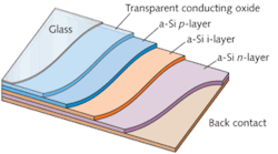
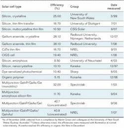
Chemical-vapor deposition forms three layers of amorphous silicon on solid or flexible substrates (see Fig. 1). Conversion efficiency can reach about 10% in the laboratory (see table). However, reaching such high efficiency requires time-consuming and painstaking batch processing. Commercial processes with high throughput yield cells with only 6% to 8% efficiency.
Amorphous silicon contains hydrogen and has a bandgap of 1.7 eV, much larger than the 1.1 eV of crystalline silicon. The larger bandgap puts peak absorption of amorphous silicon closer to the peak of the solar spectrum, increasing the energy it can extract from short-wavelength photons at the cost of reducing response to longer wavelengths. Adding germanium can reduce the bandgap closer to that of crystalline silicon. The technology is well-developed commercially, with major installations planned. OptiSolar (Hayward, CA) has announced plans to use amorphous silicon in the 550 MW Topaz Solar Farm in San Luis Obispo County, California. Construction is to start next year, with power generation to start in 2011, and the full 9.5-square-mile facility to be operating by 2013.
Polycrystalline silicon also can be deposited in micrometer-scale thin films on glass, with conversion efficiency of 7% to 8%. CSG Solar (Thalheim, Germany) produces the cells, and has reported laboratory efficiency to 10.5%.
Cadmium telluride (CdTe) is the most developed of a family of II-VI semiconductors. Its bandgap is 1.45 eV, so it can extract more energy from short-wavelength photons than crystalline silicon, at the cost of reduced response to longer wavelengths. Commercial CdTe solar cells from companies such as First Solar (Tempe, AZ) have efficiency of 9% to 10%, but laboratory efficiency has reached 16.7%. FirstSolar CdTe solar cells are being installed at the 40 MW Waldpolenz Solar Park in Germany, to be completed this year.
Efficiency of mass-produced CdTe should increase to 12% to 14% in the next few years, says Peter Peumans of Stanford University (Stanford, CA). However, cadmium compounds pose serious toxicity problems that could raise concerns for widespread application. Two early CdTe developers, BP Solar and Matsushita, both cited environmental issues when they dropped the technology earlier in this decade.
The highest laboratory efficiency yet measured for a thin-film solar cell is 19.4%, achieved at the National Renewable Energy Laboratory (Golden, CO), with copper indium gallium diselenide (CIGS), a chalcogenide with chemistry similar to II-VI compounds such as CdTe. Approaching crystalline-silicon efficiency has created “quite a bit of buzz” for CIGS, says Peumans, and startups Solyndra (Fremont, CA) and Nanosolar (San Jose, CA) are developing it commercially. But early commercial cells won’t match the laboratory efficiency, and developers need to combine the four elements in exactly the right ratios to get the peak efficiency. The availability of adequate supplies of indium could be a long-term issue.Multijunction solar cells
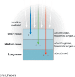
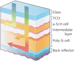
The highest conversion efficiencies to date–just over 40%–have come from stacking multiple junctions of materials with different bandgaps to collect light across the solar spectrum and into the infrared. The top layer absorbs the shortest wavelengths and transmits longer ones to lower layers, and the next highest layer then absorbs the next-shortest band (see Fig. 2). Absorption losses can be reduced by separating the bands with filters and focusing them onto separate cells, but that approach increases optical complexity.Multijunction cells have been developed using various materials, some of which are listed in the table. For example, a layer of high-bandgap amorphous silicon can be stacked on a lower layer doped with germanium to reduce the bandgap. Alternatively, microcrystalline silicon could be used as the lower layer. Multijunction cells can increase silicon thin-film efficiency from the 6% to 7% of single layers to 8% to 10% (see Fig. 3). Kaneka and Sharp (both Osaka, Japan) manufacture multijunction silicon cells.
Much higher efficiencies are possible by stacking III-V junctions and germanium. Spectrolab (Sylmar, CA) has reached 32% efficiency with layers of gallium indium phosphide (GaInP), gallium arsenide (GaAs), and germanium (Ge) at normal solar intensity. Spectrolab reached 40.7% efficiency by focusing concentrated sunlight on similar cells, and offers commercial triple-junction cells with efficiency to 28.3%, but the National Renewable Energy Laboratory holds the laboratory record with 40.8% efficiency for multilayer cells of GaInP, GaAs, and GaInAs.
The high efficiency of multijunction cells comes at a serious cost premium, which can be justified for powering a costly satellite, but not for solar-energy farms. Technical issues remain, including the high cost of depositing transparent conductive layers of zinc oxide between the junctions. Peumans has developed a technique to deposit a transparent mesh of silver nanowires, which he says reduces the cost of the transparent electrode by an order of magnitude, promising lower-cost multijunction cells.
Organic thin films
The initial appeal of organic solar cells was their potential low cost, which developers had hoped would make efficiency as low as 5% acceptable. Yet other solar power system costs, including installation, mounting equipment, and voltage inverters, make higher efficiency essential, says Peumans.
Developers are working on ways to tailor bandgaps, absorption spectra, and electronic properties of the materials. Last December last year, Konarka (Lowell, MA) reported achieving 6% efficiency with its polymer solar cell. It had earlier reported operation of flexible organic thin-film solar cells for more than a year on a rooftop with little or no degradation–a key issue for organic materials used outdoors. The company is part of a consortium hoping to reach 10% efficiency within a few years.
Meanwhile, Peumans is adapting organic pigments developed for automotive paints for use in solar cells. “Modern paints will survive more than 10 years in severe conditions,” he says, and the molecules are semiconductors that absorb visible light, making them suitable for solar cells.
Organic thin films also could be used in multijunction cells. They won’t match the 41% efficiency record of inorganic semiconductors, says Alberto Salleo of Stanford, but would be much cheaper to make because they don’t require costly molecular-beam epitaxy. “If you can get to 15% efficiency at a few tens of cents per square millimeter, there’s a big advantage.”
Other approaches and outlook
Other approaches also are in development. One is the dye-sensitized solar cell, in which dye molecules absorb light and transfer charge carriers to a solid or liquid electrolyte that acts as a semiconductor. The details are complex, but the raw materials are inexpensive and production does not require elaborate apparatus.2 Laboratory cells appear robust, and Sharp has achieved efficiency to 10.4%.
Some observers warn that thin-film solar cells may be limited to niche applications because of issues including low efficiency, poor environmental stability, and manufacturing problems. “Efficiency will be a killer, unless they can keep module production uniform and keep [efficiency] to 11% to 12%,” warns Henry Brandhorst of Auburn University (Auburn, AL). He believes China’s rapid scaling up of silicon production will cut prices and provide the raw material needed for efficient crystalline-silicon cells to continue dominating the market.
Thin-film developers remain optimistic, but Brandhorst has a point. Efficiency is hard to increase without shifting to elaborate multijunction solar cells, and without significant breakthroughs. Nonetheless, the solar-power industry is growing fast enough to support multiple technologies. Photovoltaic arrays are sprouting on rooftops and private investors and government agencies are pouring money into photovoltaic research, development, and manufacturing. The economic meltdown may leave some potholes in the road, but that won’t stop an industry on a roll.
REFERENCES
- M.A. Green, J. Materials Sci.: Materials Electron. 18, p. 515 (2007).
- F.O. Lenzmann and J.M. Kroon, Advances in OptoElectronics 2007, doi:10.1155/2007/65073.
- M.A. Green et al., Prog. in Photovoltaics Res. and Applic. 17, p. 85 (2009).

Jeff Hecht | Contributing Editor
Jeff Hecht is a regular contributing editor to Laser Focus World and has been covering the laser industry for 35 years. A prolific book author, Jeff's published works include “Understanding Fiber Optics,” “Understanding Lasers,” “The Laser Guidebook,” and “Beam Weapons: The Next Arms Race.” He also has written books on the histories of lasers and fiber optics, including “City of Light: The Story of Fiber Optics,” and “Beam: The Race to Make the Laser.” Find out more at jeffhecht.com.


