PHOTONIC CRYSTALS: Light is coupled efficiently into slow-light waveguide

One of the easier ways to achieve "slow light"—the propagation of light at a group velocity much lower than is usual in an optical material—is to use a properly configured photonic-crystal waveguide (PCW). This is fortunate, because slow light is useful in modulators, optical signal processing, optical switches, and sensing, which all benefit from the small size of PC-based devices.
But light is not easy to couple into a slow-light PCW; the mismatch in group velocity outside and inside the PCW makes coupling very inefficient. Attempts have been made to overcome this problem, but they all suffer from one or more problems, including low coupling efficiency near the band edge, narrowband performance, large physical size, and so on.
Theory and simulations have shown that adiabatic (slowly changing index) strip waveguides can efficiently couple light into and out of PCWs over the entire guided-mode spectrum; now, researchers at the University of Texas at Austin and Omega Optics (both in Austin, TX) have turned theory into practice, demonstrating optical coupling into a PCW at a high efficiency that is independent of the guided mode's group velocity.1
Couplers are eight periods in length
The PCW itself consists of a hexagonal array of air holes in silicon containing a line defect (a linear region without holes that passes entirely through the array). The lattice constant is 405 nm, the air-hole diameters are 180 nm, and the thickness of the silicon slab is 230 nm. The guided mode of the PCW includes wavelengths between 1522 and 1567 nm.
The adiabatic input and output couplers consist of PC areas with the same geometry (hex array with line defect) and lattice constant, but with holes that range in size from 180 nm at the PCW itself down to 144 nm at the outer edge of the couplers, with hole size a nonlinear function of distance from the PCW. The input and output tapers are each very short—only eight periods in length. For an experimental control, the researchers created a similar device but without the varying hole diameter. Fabricated using electron-beam lithography, the PCW with tapers and the control PCW have hole diameters and other dimensions accurate to better than 2 nm; the sidewall roughness of the holes is about 5 nm.
To characterize coupling efficiency as a function of wavelength, a TE-polarized broadband amplified-spontaneous-emission source with an spectral output of 1520 to 1620 nm was butt-coupled to the device via a singlemode polarization-maintaining tapered lensed optical fiber with a 3 μm mode-field diameter. The transmitted light spectrum and intensity were characterized with an optical-spectrum analyzer having a 0.04 nm resolution.
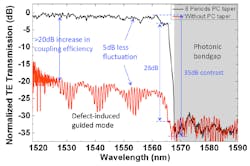
The tapered-coupler PCW performed much better than the control PCW in several ways (see figure). The coupling efficiency was higher by more than 20 dB across the whole 45 nm guided-mode bandwidth, and the Fabry-Perot noise, which manifests itself as a fine-scale fluctuation in transmission, was vastly reduced. And the transition from bandpass to bandgap cutoff was much sharper in the tapered-coupler device; this means that slow-light modes near the band edge are much more efficiently coupled with the tapered-coupler geometry.
REFERENCE
1. C.-Y. Lin et al., Appl. Phys. Lett., 97, 183302 (2010).

John Wallace | Senior Technical Editor (1998-2022)
John Wallace was with Laser Focus World for nearly 25 years, retiring in late June 2022. He obtained a bachelor's degree in mechanical engineering and physics at Rutgers University and a master's in optical engineering at the University of Rochester. Before becoming an editor, John worked as an engineer at RCA, Exxon, Eastman Kodak, and GCA Corporation.