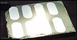
Researchers at the Lawrence Berkeley National Laboratory (LBNL; Berkeley, CA) and the University of California at Berkeley (UC-Berkeley) have developed a hybrid solar cell that combines nanotechnology with plastic electronics.1 The semiconductor-polymer photovoltaic device is expected to be cheaper and easier to make than current semiconductor devices, and may eventually provide competitive energy-conversion efficiencies (see figure).
Unlike the complex and costly fabrication of semiconductor-based solar cells, plastic solar cells can be made in bulk quantities for a few cents each. The efficiency with which plastics convert light into electricity has been poor compared to semiconductor cells, however.
"The advantage of hybrid materials consisting of inorganic semiconductors and organic polymers is that, potentially, you get the best of both worlds," said Janke Dittmer, a staff scientist at LBNL. "Inorganic semiconductors offer excellent, well-established electronic properties, and they are very well-suited as solar cell materials. Polymers offer the advantage of solution processing at room temperature, which is cheaper and allows for using fully flexible substrates such as plastics."
In a plastic solar cell, the two poles are made from hole-acceptor and electron-acceptor polymers. The Berkeley researchers used the semicrystalline polymer known as poly(3-hexylthiophene), or P3HT, for the hole acceptor or negative pole, and nanometer-sized cadmium selenide (CdSe) rods as the positive pole. "We chose P3HT because it can be processed in solution and has been used by many research groups around the world who are working on plastic transistors," said Wendy Huynh, a graduate student at UC-Berkeley. "Also, it is the conjugated polymer with the highest hole mobility found so far."
The CdSe rods measured 7 nm in diameter and 60 nm in length. Using rod-shaped nanocrystals rather than traditional spheres provided a directed path for electron transport to help improve solar-cell performance, enabling the hybrid device to achieve a monochromatic power-conversion efficiency of 6.9%, one of the highest ever reported for a plastic photovoltaic device, according to research team leader Paul Alivisatos.
The Berkeley researchers prepared their solar cells by codissolving the nanorods with the P3HT and spin-casting the hybrid solution onto a glass substrate. Keeping the length of the rods constant while modifying the diameter enabled them to tune the absorption spectrum of the cells to overlap with the solar emission spectrum. This not only enabled their hybrid cells to collect more light than typical plastic solar cells, but it also opens the door for high-efficiency devices in the future, such as tandem solar cells.
The efficiency of the hybrid cells for converting sunlight into electricity (1.7% at a 41.8° sun-horizon angle) fell far below the best semiconductor solar cells, but Dittmer expects to close that gap with time.
"The most important step is to increase the amount of sunlight absorbed in the red part of the spectrum, which we can do by going to other semiconductor materials such as cadmium telluride," he said. "Also, our published hybrid solar cells have a very simple structure, in order to investigate the science behind them. In the future, many engineering tricks can be applied to make the cells more efficient."
REFERENCE
1. W. U. Huynh, J. J. Dittmer, and A. P. Alivisatos, Science 295(5564), 2425 (March 29, 2002).
About the Author
Hassaun A. Jones-Bey
Senior Editor and Freelance Writer
Hassaun A. Jones-Bey was a senior editor and then freelance writer for Laser Focus World.
