Researchers at the National Institute for Standards and Technology (NIST; Boulder, CO) have developed an electro-optic technique for precisely calibrating photodiode frequency responses up to 110 GHz.
Sampling fast-frequency responses electro-optically is not new, according to Tracy Clement, lead author on a paper that has been accepted for presentation at the IEEE/LEOS meeting this fall. But by developing a carefully calibrated measurement, the NIST researchers have fabricated a precise metrology tool for calibrating other electrical and optical metrology equipment at frequencies about two times higher than were feasible before.
"A calibrated photodiode is a wonderful thing," said Dylan Williams, a member of the NIST research team led by Paul Hale, high-speed measurements project leader in the sources and detectors group at NIST. Williams added that vendors have already contacted the researchers about characterizing photodiodes that in turn can be used for calibrating lightwave component analyzers and oscilloscopes that would ultimately be used by companies developing communication systems.
Existing photodiode-calibration methods include the heterodyne method, which has a fairly high uncertainty above 50 GHz, and an oscilloscope, which only recently became available at bandwidths above 50 GHz, according to Hale. But digital communication equipment needs to be characterized at frequencies several times faster than its intended bit rate.
"Digital communications is basically a time-domain problem that is concerned with fast pulses in the communications system, and these pulses also have a lot of bandwidth in the frequency domain," Hale said. "If you want to reconstruct a time-domain picture of the waveform from frequency-domain information, you need to have a lot of frequency-domain information—a lot of bandwidth in the frequency domain—to get an accurate reconstruction. In the case of 40 Gbit/s, characterizing the system up to 90 GHz or more is necessary for accurately modeling the system."
Accurate measurements
In addition to providing frequency-domain measurements up to 110 GHz, the electro-optic sampling method developed at NIST has also been calibrated based on fundamental physical principles. "So we know what the bandwidth of our measurement is," Hale added. "We can do all of the corrections, and we can calculate the uncertainty in the measurement very accurately."
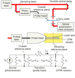
Ultrafast laser pulses stimulate photoreceiver and measure electronic output pulse via electro-optic effect on a co-planar waveguide as shown schematically from side (top), from top (center) and in electrical equivalent circuit (bottom).
null
The device uses 100-fs, 1550-nm laser pulses to optically stimulate a photodiode and to sample its electrical response on a coplanar waveguide using the electro-optic effect (see figure). The coplanar waveguide was printed on a lithium tantalate substrate. A major obstacle for the research team consisted of accurately characterizing the effects of the microwave transition from the coaxial connectors on industry devices into the planar geometry of the waveguide.
"There are lots of reflections inside of the probe, between the probe and thing you are connected to, and on the wafer itself. In addition, there is also some dispersion that we don't understand very well," Williams said. "But the probe, even without the reflections, distorts the signal as it passes through. So none of these are ideal components. There is a considerable amount of loss in the transmission lines on the wafer, which changes the relationship between the voltage and the current as it propagates in the transmission lines on the wafer."
Correcting for these numerous distorting influences involved characterizing the device with a calibrated vector-network analyzer, and then deriving an electrical-equivalent circuit. The equivalent circuit allows the behavior of the electro-optic sampler to be analyzed in terms of fundamental principles, thereby enabling measurements to be taken virtually independent of systemic effects such as signal reflections and losses.
"People have been measuring those voltages on that wafer for the last 20 years, but they haven't figured out how that voltage depends upon what is hooked up to the transmission line," Williams said. "What we've been able to do, in part at least, is work out all of what's going on electrically so that we can actually take that voltage and transform it to something that just has to do with the photoreceiver. And we can do that for any termination on the wafer."
Good linearity
The system has also demonstrated significantly improved linearity than other high-speed measurement systems. "A lot of the things we're talking about measuring are not particularly linear, so you need a linear system to be able to see the nonlinearities," Clement said.
Currently, the 110-GHz bandwidth connector is one of the few remaining limitations on the measurement bandwidth; the researchers hope to eventually get beyond that by integrating the measurement onto the wafer. But, while speed is an important factor, the primary achievement has been the development of the calibration system.
"We calibrate the impedance of the transmission line and also measure a voltage and calibrate that voltage," Hale said. "Given the impedance and the voltage we can measure current on the transmission line as well. So, as far as characterizing circuits, we have a complete characterization that we don't think anyone anywhere else has achieved."
