SHG lights path toward molecular electronics

As semiconductor devices get smaller and smaller, the silicon dioxide layers at junctions get thinner and increasingly susceptible to breakdown due to electron tunneling. So a lot of research is directed toward developing organic dielectrics with improved resistance to electron tunneling. Using funding from the National Science Foundation, researchers at the University of Pittsburgh (Pittsburgh, PA) are finding nonlinear optical techniques such as second harmonic generation (SHG) useful in this research because of its sensitivity to charging at surfaces.
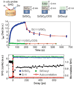
Second harmonic generation deviates from its normal quadratic variation with power at surfaces in the presence of electrical charging because of electron tunneling and trapping, according to a hypothesis advanced by the Pittsburgh researchers. They've tested the hypothesis by removing the oxide entirely and putting down another chemically passivating surface—hydrogen, which is also used in semiconductor device processing—and the quadratic behavior was restored.1 The problem with hydrogen, even though it stops the surface from reacting, is that it is not stable and will ultimately oxidize after some time in ambient air.
The next step for the researchers was to investigate how the use of a more stable passivating layer on top of the oxide might affect electron tunneling. So they grew an organic monolayer on top of the oxide, and showed that the monolayer basically stopped the charging and trapping behavior.2 They hypothesized that the 2-nm-thick layer of molecules drew its effectiveness from blocking gases from reaching the oxide surface that are believed to assist in the trapping of charges.
"We're basically looking at the semiconductor-dielectric interface and trying to devise ways of replacing the oxide with organic molecules in order to overcome this tunneling problem, and we are making a step toward molecular electronics," said Eric Borguet, an assistant professor and leader of the research team. "We are using optics to do this because nonlinear optics have the advantage of being very sensitive to electric fields at interfaces. Optics also offer potentially high resolution, real-time investigation, and spectroscopic sensitivity."
Most people think of molecular electronics in terms of molecules performing the logic operations in device circuits. But Borguet's team wants to use the molecules to replace silicon dioxide. "We are keeping the semiconductor but we are replacing the oxide with an organic layer," he said.
So far they have removed the oxide and put down molecules that bond directly to the silicon to make the silicon carbon bonds. Now they are evaluating stability and are finding the organic monolayers much more stable than hydrogen terminated circuits. In addition, the organic monolayers appear to be competitive with the silicon oxides in electrical passivity, preventing recombination of electrons and holes at the interface (see figure).
The researchers do expect to encounter problems with the organic monolayers in the manufacturing environment, however. For instance, while it is possible to heat silicon dioxide to very high temperatures (more than 1000°C) without decomposing, organic monolayers cannot be heated to such high temperatures.
"There are processing steps in industry that require very high temperatures and the organic monolayers may not be suitable," Borguet said. "But I think that there are ways to get around that. Not all devices require those high-temperature processing steps."
Alternative semiconductor materials
Potential applications of the organic monolayer interfaces include functionalization of molecules (in which dipoles or receptors may be placed on molecules to form semiconductor-based sensors) and passivation of alternative semiconductor materials such as germanium, which offers better charge mobility than silicon.
"The first semiconductor transistor was made of germanium, but the reason that we have Silicon Valley instead of Germanium Valley is due in large part to the fact that the oxide that forms on germanium is soluble in water. Fortunately, silicon dioxide is glass and is insoluble in water. So we make a much better interface between silicon and silicon dioxide than we can with germanium and germanium dioxide. Perhaps we can replace germanium dioxide with other inorganic layers or with an organic layer and regenerate interest in germanium devices," noted Borguet.
To further their research, Borguet's team is collaborating with other researchers at the University of Pittsburgh to build a photoemission electron microscope that will help them to observe the emission of electrons from surfaces at very high spatial resolution.
"We're going to be looking at these charge-tunneling and trapping issues, but with much higher resolution," he said. "We'd like to be able to turn this technique into a kind of second harmonic microscopy."
REFERENCES
1. V. Fomenko, J.-F. Lami, and E. Borguet, Physical Rev. B(63), 121316-1.
2. V Fomenko et al., J. Appl. Phys. 91(7), 4394 (April 1, 2002).
Hassaun A. Jones-Bey | Senior Editor and Freelance Writer
Hassaun A. Jones-Bey was a senior editor and then freelance writer for Laser Focus World.