FREE-ELECTRON LASERS: FLASH forward to another record

The FLASH (Free Electron Laser in Hamburg) facility at the DESY research center in Germany (www.desy.de) has beaten its own record as the source of the lowest wavelength free-electron-laser (FEL) pulses, halving the previous record to just 6.5 nm.
The facility has long been the premier source of ultrafast, FEL pulses, growing out of TESLA, a 55-institute, 12-country collaboration started in 1991 to develop low-cost accelerator sources based on superconducting cavities as opposed to the traditional, expensive copper cavities. The success of the electron/positron collider that became the TESLA Test Facility was quickly seen as a possible new light source; researchers planned to upgrade the accelerator and add a number of undulators-cavities with alternating magnetic fields that manipulate the group velocity of the electron bunches such that laser pulses are formed. Taken together, an ultraviolet, ultrafast laser was born. First lasing of the new technology was shown in 2000, at 100 nm, and the facility was renamed FLASH, with new records coming at intervals as regular as the pulses.
The FEL facility has been undergoing an upgrade over the past several months, including a lengthening of the linear accelerator by 12 m and the addition of a sixth superconducting undulator. On Oct. 5, the facility measured its ultimate design wavelength of just 6.5 nm.
New center to host FEL research
The record comes about as the Center for Free-Electron Laser Science has come into being, a consortium that includes the University of Hamburg, the Max Planck Society, the City of Hamburg and DESY. The center has been funded with €50 million ($72 million) from Hamburg and will house around 300 scientists when the building at DESY is completed in 2010.
Jochen Schneider, DESY research director, has a long list of the science that will be enabled by FLASH. “Individual atoms, molecules, viruses, clusters and in general nanosize particles can be studied on the fly,” Schneider says, “because we get in flashes of 10 fs duration as many photons as the best synchrotron radiation facilities get per second.” That opens up studies on multiphoton processes on atoms and clusters, a variety of two-color pump-probe experiments in the infrared and the soft x-rays or their harmonics, characterization of volume plasma and study of ablation processes, time-resolved photoelectron spectroscopy, and time-resolved photoelectron spectroscopy, to name just a few. The fundamental limitation, clearly, is beam time; applications for use of the facility exceeded available beam time before the upgrade even occurred.
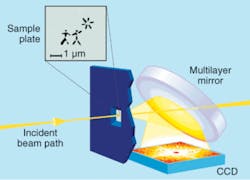
The flashes from FLASH will yield higher resolution than longer exposures from, for instance, synchrotron sources, where radiation damage limits the ultimate resolution. Last year, Lawrence Livermore Laboratory’s Henry Chapman showed that a single shot from FLASH yielded a diffraction image in the instant before the sample turned to plasma, a promising result for the molecular-scale femtosecond flashbulb that free-electron lasers have promised for so long. Chapman will now go on to lead an experimental group at DESY. “Reaching 6 nm was a tour de force of engineering and control, he says.” And 6.5 nm is not even the end of the line; harmonics of the pulses can be put to use as well. “The third harmonic of FLASH at 6 nm is 2 nm,” Chapman says. “Even though the third harmonic is less than 1% of the fundamental, this is still the highest peak brightness of any source in this wavelength range by many orders of magnitude.”
While FLASH will certainly hold these records for some time to come, other x-ray FELs are being built around the world. Japan is building Spring-8, a prototype for a hard-x-ray FEL, which is coming online this month at a design wavelength of 49 nm. Another project called LCLS at the Stanford Linear Accelerator (www.slac.stanford.edu) will provide 0.15 nm x-rays and should come online in mid-2009. But most important, just around the corner from FLASH is the XFEL project, a 3.4-km-long FEL that will provide 0.1 nm x-rays (xfel.desy.de).
Massimo Altarelli, European Team Leader of XFEL, says that the successes at FLASH are important milestones for the development of the production and detection technologies for the XFEL. “FLASH is a huge prototype that validates all the basic components of the future XFEL: the gun, the injector, the accelerating modules, and so on. It also provides an excellent testing ground for all experimental protocols that are going to be used on XFEL and an opportunity to learn how to handle subpicosecond extremely brilliant bursts of x-rays. It is hard to imagine a better validation of the basic technology and of the components of the XFEL.”
D. Jason Palmer | Freelance writer
D. Jason Palmer is a freelance writer based in Florence, Italy.