PHOTONIC FRONTIERS: NANOPHOTONICS - Nanophotonics is a matter of confinement

Nanophotonics is a hard field to pin down because it means different things to different people. At a fundamental level, nanoscale devices should have dimensions measured in nanometers, a broad range from 1 to 999 nm that includes the nominal size of visible photons. But size isn’t the whole story-nanoscale devices function by confining something on a nanometer scale, and fall into two broad categories.
One family of devices confines current carriers on a nanometer scale. Quantum wells have done that for a long time, starting before nanotechnology became a hot buzzword. Quantum wells confine carriers in one dimension, quantum wires confine them in two dimensions, and quantum dots confine carriers in three dimensions. The confinement is on the scale of the de Broglie wavelength of electrons in the valence band of a semiconductor, about 50 nm, and these electrons interact with photons, which are much larger.
A second, newer, family of nanophotonic devices confines visible and infrared photons rather than carriers. The scale of confinement is determined by internal structures such as photonic crystals, which are wavelength-selective. Photonic confinement can create novel cavities, waveguides, and other devices, and enhance optical and nonlinear interactions.
Quantum wells, dots, and boxes
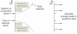
A quantum well is essentially a very thin version of a semiconductor double-heterostructure diode. If the thickness of the middle layer is reduced below 50 nm, quantum effects dominate over bulk semiconductor properties, creating discrete subbands in the valence and conduction bands in the middle layer, where carriers are trapped because it has a smaller bandgap. With confinement only in one dimension, energy levels approximate those in bulk material. A quantum dot of small-bandgap material confines the carriers in all three dimensions, restricting energy to discrete levels (see Fig. 1).
Quantum dots in the junction layer of a diode can function as lasers and LEDs (light-emitting diodes). Recombination of carriers produces emission at sharply defined wavelengths depending on size of the dots as well as their composition. Early developers had hoped quantum-dot lasers would be more efficient than quantum-well devices, but in general quantum-dot lasers have not worked very well, says Dan Botez of the University of Wisconsin in Madison. Although quantum-dot lasers have low thresholds, they can’t hold onto carriers well at the high carrier densities needed for laser action. “You lose up to 80% of the carriers by the time you get to threshold,” Botez says.
To avoid the high carrier losses, Botez is etching confinement structures individually into the semiconductor to create quantum boxes.1 As in quantum-cascade lasers, the goal is to operate on transitions between subbands of the conduction electrons, rather than on bandgap transitions. Although etching tends to produce surface defects, the transitions are at energies of a fraction of an electron volt, with energy too small to see the defects. Botez has observed emission but has yet to demonstrate laser oscillation.
Other quantum-dot devices
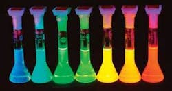
Although quantum dots do not lase well, they can be used as LEDs. Optical pumping is particularly effective, and quantum dots dispersed in a liquid fluoresce brightly under ultraviolet illumination. The emission wavelength increases with size, so size selection gives different colors (see Fig. 2).Quantum dots have carrier recovery times 10 to 100 times faster than conventional semiconductor optical amplifiers, making them very attractive for high-speed amplification. Researchers at the University of Toronto (Canada) have observed recovery times as fast as 15 ps at 1560 nm in indium gallium arsenide phosphide (InGaAsP) quantum dots, which they consider fast enough for switching at rates higher than 40 GHz.2 In addition, quantum dots saturate easily, making them attractive for switching and modelocking.
Nanostructures are also being studied for sensing, photovoltaic energy production, and photodetectors. The dependence of quantum-dot energy levels on their size allows fabrication of quantum dots tailored to absorb specific wavelengths, potentially increasing energy conversion of photovoltaics. Quantum dots also can be dispersed in carrier materials, to increase energy collection efficiency. Another novel application is an avalanche photodiode made at Harvard University from crossed nanowires of silicon and cadmium sulfide; it can detect less than 100 photons and offers 250 nm spatial resolution.3
Nanoscale optical confinement
The confinement of photons in a nanoscale optical cavity offers other possibilities. The spontaneous emission rate depends on cavity properties, increasing with Q factor and decreasing with mode volume. Photonic-crystal cavities can be made with model volumes smaller than the cube of the wavelength (measured as the wavelength λ in air divided by refractive index n of the medium). They also can be fabricated with high Q factors. Together that greatly enhances the spontaneous-emission rate and the fraction of those photons coupled into a single-cavity mode. This allows a single nanocavity to operate as a laser with a very low threshold. A team at the Korea Advanced Institute of Science and Technology (Daejeon, South Korea) has demonstrated threshold of about 260 µA for an electrically pumped photonic crystal with a single with modal volume only 0.684 (λ/n)3.4 Such devices can be attractive as single-photon sources, but their output power is too low for many other applications.
Assembling two-dimensional arrays of coupled photonic-crystal nanocavities can generate higher powers. At Stanford University (Stanford, CA), Hatice Altug and Jelena Vuckovic made nanocavity arrays in an indium phosphide structure with four InGaAsP quantum wells in the active layer (see Fig. 3). Optically pumping the 9 × 9 array, they observed single-mode output with a threshold about 10 times higher than for pumping a single cavity. However, the researchers believe they can extract more power per cavity in their array than they could from a single cavity.5 Both single and array nanocavities have extremely fast response times, with direct modulation of an optically pumped single cavity possible at speeds faster than they could record with a 100 GHz detector.6Nanocavities can be reduced to even smaller modal volumes by adding discontinuities smaller than a wavelength to shrink local field strength, according to a theoretical study by Michal Lipson’s group at Cornell University (Ithaca, NY). The group calculates the cavity volume could be made as small as 0.01 (λ/2n)3 a dimension they chose to emphasize that volume is much smaller than the classical diffraction limit of roughly a half wavelength. The researchers say their approach should increase output power and nonlinear effects in most types of microcavities.7
Lipson also is working on a new slot design for a subwavelength metallic waveguide with attenuation of 0.8 dB/µm, much less than the 30 dB/µm typical of earlier designs. The key to reducing loss is sandwiching a dielectric layer between metal cladding layers separated by as little as 150 nm.8 Her group also used a silicon slot waveguide fabricated as a loop to make an unusual emitter that was electronically pumped by a cathode inside the loop and an anode outside.9
Outlook
Like other types of nanotechnology, nanophotonics is in the early stages of exploring possibilities, and some ideas have been studied much more than others. This article has barely scratched the surface.
Considerable effort has gone into exciting emission from quantum dots and more recently from nanocavities, but important refinements continue. In June, a team from the University of Tokyo reported what it said was the first room-temperature continuous-wave lasing at 1.3 µm from a photonic-crystal nanocavity using a quantum-dot active layer.10 The group reported stable optical output when the optical pump power was just above threshold, but found that long-term pumping at 1.5 times the threshold could damage the cavity, a sign much development remains.
Many other ideas are still emerging. Can the intense concentration of optical fields in the tiny volume of a nanocavity be tapped to enhance nonlinear effects? How can photonic crystals manipulate light? How can optical signals be coupled in and out of nanophotonic devices? A tremendous amount remains to be learned for technologists to be able to pick the most promising ideas and implement them.
REFERENCES
1. D. Botez, Laser Physics 15, 966 (2005).
2. A.J. Zilkie et al., Optics Express 14, 11453 (Nov. 13, 2006)).
3. O. Hayden et al., Nature Materials doi: 10.1038/nmat1635 - online publication (April 16, 2006).
4. H.-G. Park et al., Science 305, 1444 (Sep. 3, 2004).
5. H. Altug and J. Vuckovic,IEEE LEOS Newsletter, Apr 2006, p. 4 and H. Altug and J. Vuckovic, Optics Express 13, 8820 (2005).
6. H. Altug et al, Nature Physics 2, 484 (July 2006).
7. J.T. Robinson et al., Phys. Rev. Lett. 95, 143901 (2005).
8. L. Chen et al., Optics Letters 31, 2133 (July 2006).
9. C.A. Barrios and M. Lipson, Optics Express 13, 10092 (Dec. 12, 2005).
10. M. Nomura et al., Optics Express 14, 6308 (June 26, 2006).

Jeff Hecht | Contributing Editor
Jeff Hecht is a regular contributing editor to Laser Focus World and has been covering the laser industry for 35 years. A prolific book author, Jeff's published works include “Understanding Fiber Optics,” “Understanding Lasers,” “The Laser Guidebook,” and “Beam Weapons: The Next Arms Race.” He also has written books on the histories of lasers and fiber optics, including “City of Light: The Story of Fiber Optics,” and “Beam: The Race to Make the Laser.” Find out more at jeffhecht.com.

