SHORT-WAVE DIODE LASERS: Nonpolar gallium nitride laser diodes are the next new blue
Daniel Feezell, Shuji Nakamura, Steve DenBaars, and Jim Speck
Despite their relatively young age, blue-violet gallium nitride (GaN)-based laser diodes have achieved remarkable progress since their first demonstration in 1996. Development of epitaxial growth techniques, defect-reduced substrates, and sophisticated device design has resulted in high-performance lasers with commercial viability. These devices have already emerged as critical components in the next generation of DVD players, such as Blue-ray Disc and HD-DVD, and have generated considerable interest in applications such as projection displays, high-resolution printing, and optical sensing.
However, despite their significant success, conventional GaN-based laser diodes suffer from an inherent limitation-internal polarization-related electric fields that limit their optical efficiency. To address this fundamental issue, our research group at the University of California, Santa Barbara (UCSB), has been investigating GaN-based laser diodes grown on nonpolar crystal planes, which are free from polarization-related electric fields. With rapid progress already occurring on these alternative structures, nonpolar GaN-based laser diodes are emerging as a promising alternative to their polar c-plane counterparts.
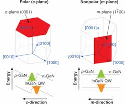
Conventional GaN-based laser diodes are grown on the c-plane of the würtzite crystal, leading to spontaneous piezoelectric polarization within the heterostructure.1 These polarization effects generate electric fields that distort the InGaN quantum wells (QWs) into a triangular shape and spatially separate the electron and hole wavefunctions, thus reducing their radiative recombination efficiency (see Fig 1). For electrically injected laser diodes, extra carriers are required to screen these electric fields and flatten the distorted energy bands before efficient gain is provided. This process translates into increased threshold current densities for the lasers.
Furthermore, c-plane structures typically require thin (less than 4 nm) QWs to alleviate these polarization-related problems (which become enhanced for greater QW thicknesses). This requirement places several restrictions on the optical design of c-plane GaN-based lasers. One example is the inclusion of thick aluminum (Al)-containing waveguide cladding layers, such as AlGaN/GaN superlattices, which are required to provide transverse optical-mode confinement. Unfortunately, the inclusion of thick Al-containing layers typically leads to manufacturing problems such as cracking due to tensile strain, higher-voltage operation, reduced yield, and poor reactor stability.
To address these issues, the scientific community has been developing structures grown on nonpolar planes of GaN. In contrast to c-plane laser diodes, nonpolar laser diodes are grown on the side face of the würtzite crystal; known as the m-plane. These devices are free from the polarization-related electric fields that plague c-plane structures. The energy bands of InGaN QWs grown on m-plane GaN are undistorted, resembling the more rectangular shape of conventional QWs grown on gallium arsenide or indium phosphide. These QWs do not suffer from the separation of the electron and hole wavefunctions typical of c-plane structures. Additionally, with no polarization-related electric fields present, no extra carriers are required to achieve efficient optical gain. Indeed, higher optical gain is theoretically predicted for these structures.2
The limited availability of low-defect-density substrates has been a hindrance to development of light-emitting diodes (LEDs) and laser diodes on nonpolar GaN. Initially, researchers explored hetero-epitaxial growth of nonpolar GaN on foreign substrates. Unfortunately, these films were plagued with a high density of threading dislocations and stacking faults, which act as nonradiative recombination centers and limit the optical performance of the devices. Fortunately, Mitsubishi Chemical (Ibaraki, Japan) has recently developed low-defect-density free-standing m-plane GaN substrates. These substrates are grown by hydride vapor-phase epitaxy in the c-direction and then sliced vertically to expose the m-plane. The m-plane surface is then prepared by chemical and mechanical surface treatment. The resulting substrates have threading dislocation densities of less then 5 × 106 cm-2 and have rendered efficient nonpolar GaN-based laser diodes a reality.
In February 2007, two groups at UCSB and Rohm (Tokyo, Japan) independently reported the fabrication of the first nonpolar GaN-based laser diodes.3, 4 The initial devices reported at UCSB were broad-area gain-guided lasers driven in pulsed mode, with threshold current densities of 7.5 kA/cm2. Rohm announced continuous-wave (CW) operation through the use of index-guided ridge-laser geometry. The maximum reported output power was 10 mW and the threshold current density was 4.0 k A/cm2. Both research teams fabricated their devices on material grown by metal-organic chemical-vapor deposition on free-standing m-plane GaN substrates from Mitsubishi Chemical.
AlGaN-cladding-free structures
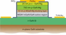
In March 2007, UCSB reported another major breakthrough for nonpolar GaN-based laser diodes-devices without any Al-containing waveguide cladding layers.5 The absence of polarization-related effects in nonpolar GaN allows for the implementation of relatively thick (greater than 8 nm) InGaN QWs in the laser diodes without a reduction in radiative efficiency. These thick InGaN QWs can provide adequate transverse optical-mode confinement in the lasers, eliminating the need for the problematic Al-containing waveguide cladding layers required in c-plane structures (see Fig 2). These AlGaN-cladding-free devices are uniquely afforded by the nonpolar structure and can be grown and fabricated much like the GaN-based LEDs, which ultimately offers a more straightforward way to manufacture GaN-based laser diodes. The only Al-containing layer in these devices is a thin (10 nm) AlGaN electron-blocking layer.
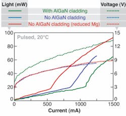
To compare the new AlGaN-cladding-free design to the more conventional GaN-based laser diode, we grew nonpolar structures with and without the AlGaN cladding and fabricated them into broad-area laser diodes. Aside from the presence of the AlGaN cladding, the basic structures of these laser diodes were the same. Both devices contained five 8-nm-thick InGaN QWs separated by 8-nm-thick GaN barriers. The light-current-voltage (LIV) characteristics of these devices were compared (see Fig. 3). The first device had a similar structure to a c-plane GaN-based laser diode, with AlGaN/GaN superlattices surrounding the active region on both sides. This structure produced a threshold voltage of 11.7 V and a threshold current density of 7.2 kA/cm2.
The second device differed only in that it contained no AlGaN cladding layers. This reduced the threshold voltage to 7.6 V and the threshold current density to 5.6 kA/cm2. The benefits of the AlGaN-cladding-free structure were immediately obvious, with the new design demonstrating significantly lower voltage and current operation. In fact, optimizing the performance of these AlGaN-cladding-free devices proved to be much more straightforward than conventional structures. The absence of thick AlGaN layers ensured consistent device performance using simple, repeatable growth and fabrication techniques.
Finally, we varied the magnesium doping levels in another AlGaN-cladding-free structure containing an active region with three 13-nm-thick InGaN QWs, to demonstrate a threshold voltage of 6.7 V and a threshold current of 3.7 kA/cm2. These broad-area devices contained uncoated, etched facets. After using a focused ion-beam tool to generate smoother and more vertical facets, the threshold current density on these broad-area lasers was reduced to less than 3.0 kA/cm2, indicating the potential of m-plane lasers with ideal mirror reflectivity. Cleaved facets along the a-direction and c-direction are possible on m-plane material and will offer the best long-term solution for smooth and vertical mirrors-a solution that Rohm and UCSB are currently developing.
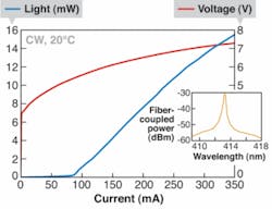
Through implementation of an index-guided ridge-laser design, our research team at UCSB recently demonstrated continuous-wave operation of AlGaN-cladding-free GaN-based laser diodes (see Fig 4). The structures were grown in a manner analogous to LEDs, contained uncoated and etched mirror facets, and employed no heat sinking. These devices had threshold current densities of 5.4 kA/cm2, threshold voltages of 5.4 V, and a lasing wavelength of 413.3 nm for a 1.9 × 800 µm ridge, and a characteristic temperature (T0) of 86 K (see Fig. 5). We operated these laser diodes CW under ambient conditions at a constant current of 175 mA for more than 15 hours, which we expect will be significantly longer with optical-facet coatings and packaging.
null
While the demonstration of CW operation somewhat validates the potential of the AlGaN-cladding-free design, these devices are far from optimized. For example, the threshold current densities of the CW ridge lasers (5.4 kA/cm2) do not yet reflect the performance of our broad-area laser diodes at 3.0 kA/cm2. We are currently working to improve our ridge-laser design and fabrication techniques to achieve ridge-laser threshold current densities that closely mimic those of the broad-area devices. Another area that requires immediate improvement is the low characteristic temperature (T0) of these devices. Our value is significantly smaller than that reported by Rohm and may indicate potential problems with Al incorporation in the AlGaN electron-blocking layer. Optimization of the AlGaN electron-blocking layer is currently under way.
Optoelectronic devices grown on nonpolar GaN overcome several limitations of conventional c-plane structures. The absence of polarization-related electric fields in nonpolar structures promises more efficient devices with a higher degree of design flexibility. Novel device designs unique to nonpolar GaN, such as AlGaN-cladding-free structures, may improve the manufacturability and reliability of GaN-based laser diodes. Further improvements in substrate quality and device optimization should ultimately propel these nonpolar emitters to a higher performance level that rivals that of their conventional cousins.
ACKNOWLEDGMENTS
Researchers contributing to this work at UCSB are Shuji Nakamura, Steve DenBaars, Jim Speck, Daniel Cohen, Daniel Feezell, Mathew Schmidt, Robert Farrell, Anurag Tyagi, and Kathryn Kelchner. The authors acknowledge the support of the Solid State Lighting and Display Center at UCSB and the supply of substrates from Mitsubishi Chemical .
REFERENCES
1. S. Chichibu et al., Appl. Phys. Lett. 69, 4188 (1996).
2. S.H. Park et al., Jpn. J. Appl. Phys. 42, L170 (2003).
3. M. Schmidt et al., Jpn. J. Appl. Phys. 46, L190 (2007).
4. K. Okamoto et al., Jpn. J. Appl. Phys. 46, L187 (2007).
5. D. Feezell et al., Jpn. J. Appl. Phys. 46, L284 (2007).
Tell us what you think about this article. Send an e-mail to [email protected].m.
DANIEL FEEZELL is a postdoctoral researcher, SHUJI NAKAMURA is professor, STEVE DENBAARS is professor, and JIM SPECK is department chair and professor at the Department of Materials, University of California, Santa Barbara, 93106-5050; e-mail: [email protected]. Shuji Nakamura is also director of the UCSB Solid State Lighting & Display Center.
