Last spring, as Motorola (Austin, TX) was announcing a successful demonstration of the first 4-Mbit electronic silicon nanocrystal memory device, researchers from the California Institute of Technology (Pasadena, CA), and Intel (Santa Clara, CA) were describing successful data-read operations in optical nanocrystal memory devices, ultimately intended for future all-optical communications systems, at the April meeting of the Materials Research Society (MRS) in San Francisco, CA.
Electronic nanocrystal memory has emerged as an interesting candidate for future nonvolatile memory because of desirable characteristics such as reliable and robust charge storage, hundredfold improvements in program and erase speeds, lower programming voltages, and improved compatibility with large-scale integration fabrication procedures in comparison with conventional flash memories.
Considering the potential advantages, as well as the Motorola announcement, a commercially available electrical nanocrystal memory may well be announced by a major semiconductor company within the next two years, said Harry Atwater, a principal investigator at CalTech, whose group also described a waveguide technology for optical propagation below the diffraction limit (see related story, p. 37). An optical analog to the electronic nanocrystal memory will require a good bit more development. But the basic physics as demonstrated in the CalTech-JPL-Intel work indicates that an optical memory based on reading, writing, and erase nanocrystals is certainly possible.
"The application here is aimed at future all-optical communications systems, where one would like to have an optical buffer," he said. "We are trying to use nanocrystals as a way to make an all-optical memory that could act as a buffer for packets of information in optical networks."
Reading and writing
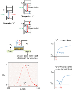
A two-state memory (left) can be set electronically and read optically through a transparent top gate (below). An optical read when current is flowing (uncharged state) yields photoluminescence at 800 nm, which is absent in the charged state.
When the optical nanocrystal is uncharged, incident light is re-emitted as photoluminescence. But the photoluminescence process is quenched in a charged nanocrystal, which results in a two-state memory system (see figure). The Atwater lab has demonstrated optical memory reading using devices imbedded in the gate stack of a transistor that are similar to electronic nanocrystal memories. But instead of having several layers of metallization and an electrical contact at the top, they have worked with collaborators at Intel to make optically transparent top gates with a 40-nm thick polysilicon top contact.
They currently program the devices electrically and read them optically at an emission wavelength of about 800 nm using an argon-ion laser. Writing the devices optically will require shining light at a higher photon energy suitable for internal photoemission, which will require engineering both writing wavelength and nanocrystal size.
"Ultimately, I imagine that a compact, relatively low-cost system would have a solid-state gallium nitride laser diode emitting at about 400 nm for writing, and a gallium arsenide light-emitting diode (LED) or laser at 800 nm for reading," Atwater said. "We are aiming at a system in a very small package, powered by, say, a 5-V power supply with these two LED or laser sources."
An interesting aspect of nanocrystal material systems is that the size regime provides engineering control over the optical properties through quantum confinement, he added. "So you're not stuck with the bandgap of silicon, which is at 1.1 eV. In fact you can have emissions basically throughout the visible and near-infrared."
A major hurdle that remains in the development process, however, lies in the relatively long emission lifetime in silicon, which may critically limit program and erase speeds. "A microsecond lifetime would mean that the device speed would be about a megahertz, which is way too low to be interesting," said Rob Walters, a member of the Atwater research team who presented another aspect of the work at the MRS meeting.
"We think that the speed may in fact be limited by the speed with which programming and deprogramming the charge in the nanocrystal can actually be performed, and that potentially could be a lot faster [than the silicon emission lifetime]," Walters said. "There are a number of fundamental questions related to how fast we can read and write. It's not yet clear that the speeds are high enough. But it's not clear that they are not either."
