Imagine one ternary material system for optical illumination smoothly spanning all wavelengths from near-infrared to deep ultraviolet. That's what basic science researchers at the Lawrence Berkeley National Laboratory (LBNL; Berkeley, CA) and numerous other places around the world are working toward with the recent revelation that the bandgap energy of indium nitride (InN) appears to be just below 0.7 eV, as opposed to the previously believed 2.0 eV.
The observation of optical absorption in InN at surprisingly low bandgap energies is 15 or 20 years old, as is the heretofore puzzling lack of photoluminescence at its supposed 1.9-eV bandgap, according to Wladek Walukiewicz, senior staff scientist in the material science division at LBNL, who led the team of researchers at LBNL, Cornell University (Ithaca, NY), and Ritsumeikan University (Shiga, Japan) who made the discovery.1, 2
The 1.9-eV bandgap had been experimentally observed in seemingly pure InN samples prepared through sputtering, so previous observations of optical absorption and even photoluminescence at lower bandgap energies were generally assumed to be artifacts emanating from localized, deep states in the material as opposed to the potentially useful illumination from delocalized bandgap states.
So Walukiewicz' team did not start out looking for illumination at 0.7 eV. Driven by a widely shared frustration at the lack of potentially useful red light emissions from InN in spite of the bright blue, green, and violet emissions of indium gallium nitride, they decided to basically "force light out of the InN," he said. "So we blasted it with lasers and we applied very high pressure. But we couldn't get anything."
Then, based on hints in the literature that optical absorption actually started at much lower energy levels, the researchers replaced their photodiodes with germanium detectors, and the germanium bandgap on the order of 0.75-eV revealed InN photoluminescence in that energy region. "Even at that point we were hesitant because of the possibility that it could be deep-level related," he said. But the observed optical absorption was strong. The researchers also observed photomodulated reflection due to free-charge carriers modulating the reflection of incident laser radiation at the band edge—a sign of band-edge absorption.
Another factor that encouraged the researchers to question the accepted 1.9-eV bandgap was the observation of an energy dependence in the electron effective mass.3 "If the gap was 2 eV, electron effective mass would be constant independent of how many electrons you have," he said.
Looking back at InN samples that had yielded the original 1.9-eV bandgap energy revealed high levels of oxygen contamination (on the order of 10% to 30%), probably resulting from the sputtering technique of knocking component atoms from a solid target using a beam of hot plasma. The LBNL samples, however, were created using the much cleaner method of molecular-beam epitaxy. Subsequent to their initial publications, the researchers have actually achieved bandgap energies below 0.7 eV by producing purer InN, and are now using indium arsenide detectors to observe the resulting photoluminescence. While skepticism at the validity of these observations remains, Walukiewicz said that other research teams have begun to replicate their results independently using other fabrication methods such as metal-oxide chemical-vapor deposition.
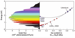
Immediate applications for this development are being pursued for production of solar cells based on indium gallium nitride (InGaN) material systems (see figure). With bandgap energies ranging from 0.7 eV for InN to 3.4 eV for GaN, this one ternary material system could span almost the entire solar spectrum from 0.4 to 4.0 eV smoothly enough to inexpensively achieve theoretical efficiency limits of solar energy generation for the first time in real-world systems. The material also potentially offers a higher level of radiation hardness for space-based applications than current solar-cell materials.
Beyond that, the group has already begun to look at ternary systems based on indium aluminum arsenide in which the 6.2-eV bandgap of AlAs could conceivably provide an optical range for a single material system that ranges from the near infrared to the deep ultraviolet.
REFERENCES
- J. Wu et al., Appl. Phys. Lett. 80(21) 3967 (May 27, 2002).
- J. Wu et al., Appl. Phys. Lett. 80(25) 4741 (June 24, 2002).
- J. Wu et al., Phys. Rev. B Rapid Communications; in press.
About the Author
Hassaun A. Jones-Bey
Senior Editor and Freelance Writer
Hassaun A. Jones-Bey was a senior editor and then freelance writer for Laser Focus World.
