FOCAL-PLANE ARRAYS: Curved sensor array to help simplify cameras
As every camera-lens designer knows, the need to produce flat image planes drives up the mass and complexity of camera optics. And the image sensors in digital cameras are, if anything, flatter than the photographic film that lens designers have been contending with for more than a hundred years. But researchers at Stanford University have taken advantage of the wonders of optical lithography to develop a monolithic but flexible silicon digital-sensor geometry that can easily conform to nonplanar contours; they have chosen the sphere (actually, a section thereof) as the contour that leads to the simplest lens designs.
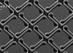
In their sensor, each pixel exists on its own little silicon island (see Fig. 1), with all pixels laid out in the usual rectilinear geometry. Each island is connected to its four neighbors only by thin silicon springs, allowing the overall pixel surface to deform as if it were a stretchable rubber sheet. For example, a prototype device made of a square array 1 × 1 cm2 in size with 105 × 105 islands (although containing no active pixels) fabricated from silicon 30 µm thick was deformed into a subhemispherical dome having a mere 1 cm radius.1
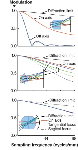
The researchers also theoretically analyzed the performance of curved versus planar arrays.2 They took the typical lens of a low-end photographic camera—a Cooke triplet—in combination with a planar focal-plane array (FPA) and compared it to a more-economical, but far-worse-performing singlet-lens/planar-FPA combination, as well as a curved FPA combined with a ball-shaped singlet lens that has the stop at its center. All three camera lenses were entirely of BK-7 glass, while the f number for all three optical systems was 3.5. The angular fields of view of the singlet, triplet, and ball-lens systems were 52°, 55°, and 69° respectively.Superior performance
Modulation-transfer-function (MTF) plots for all three systems were calculated for wavelengths of 656.3, 587.6, and 486.1 nm (red, green, and blue) and for on- and off-axis points. The singlet’s performance was only middling on-axis and terrible off-axis (see Fig. 2), while the Cooke triplet did very well on-axis and acceptably off-axis. The term “off-axis” could be considered a misnomer for the Stanford system, however, because both surfaces of its singlet lens, as well as the surface of the sensor, are all spherical with their center of curvature at the system’s stop. This lack of off-axis qualities is borne out by the system’s MTF, whose on- and off-axis theoretical plots are virtually identical (not to mention superior to the Cooke triplet’s on-axis performance, and not too far from diffraction-limited).
The flat silicon array is curved by pressing it onto a pushrod with a spherical top. There is no external method to horizontally position the pixels on the image surface. “The placement of each pixel is governed by the spring forces (all deformation is elastic) and can hence be ‘programmed’ by engineering the mask layout for optimal pixel placement by tuning of the spring widths (thicknesses) and therefore spring constants,” says Peter Peumans, on of the researchers. The resulting pixel-fill factor ranges from 75% at a corner to 30% at the center—numbers that could be raised by beginning with a different array design that takes deformation into effect.
Fabricating live pixels on the silicon islands has yet to be done, although how that will be accomplished is being planned out. “The pixels of a focal-plane array require five connections: power, ground, reset, row-select, and output,” says Peumans. “The springs that connect pixels within a row could carry three of these signals (power, ground and row-select), while the columns could carry the remaining two (reset and output). This way, selecting a row would allow for read-out at the bottom of the array. The springs would need multiple levels of metal, but that is not a problem in modern CMOS.”
While the Stanford researchers have a good idea what the chips will look like, they will need someone else to make the ICs. “We are looking for industrial partners to design the chip together and build the chip for us (pixel design, row decoders and read-out circuitry),” says Peumans. “We would do the post-processing (deep etch, undercut, and curving) and camera assembly here at Stanford. We’ve had some major camera companies express interest, but we have not yet started any formal collaborations.”
REFERENCES
1. R. Dinyari et al., Applied Phys. Lett. 92, 091114 (2008).
2. S.-B. Rim et al., Optics Express 16(7) (March 31, 2008).

John Wallace | Senior Technical Editor (1998-2022)
John Wallace was with Laser Focus World for nearly 25 years, retiring in late June 2022. He obtained a bachelor's degree in mechanical engineering and physics at Rutgers University and a master's in optical engineering at the University of Rochester. Before becoming an editor, John worked as an engineer at RCA, Exxon, Eastman Kodak, and GCA Corporation.

