PLASMONICS: Lasing spaser creates coherent radiation

A new type of nanoscale optical device called a lasing spaser combines metamaterials and spasers to create a versatile planar source of coherent radiation. The spaser (surface-plasmon laser) is a quantum amplifier of surface-plasmon emission with potential in a wide range of applications from nanoscale lithography and ultramicroscopy to ultrasensitive surface-enhanced Raman scattering. Introduced in 2003,1 the spaser is the equivalent of a laser but it amplifies plasmon resonances rather than photons, with plasmonic resonators instead of a resonant cavity.
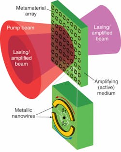
In the so-called lasing spaser conceived by Nikolay Zheludev at Southampton University (Southampton, England), a two-dimensional array exploits a slightly perturbed symmetry within its structure to emit spatially and temporally coherent radiation normal to its surface.2 The structure consists of a regular array of metallic asymmetric split-ring (ASR) resonators, which generates spatially coherent and high-quality-factor (high-Q) current oscillations. Here the high-quality factor needed for lasing and amplification is a feature of the collective “coherent” response of the whole arrayan individual ARS does not show such a high-quality response. On top of this array sits a thin substrate of amplifying dielectric material such as a semiconductor that can be optically or electrically pumped. A minor asymmetry designed into the ASR resonators breaks the trapped-mode oscillation in the amplifying substrate, causing a portion of the energy to be emitted into free space (see figure).3
Zheludev and his group considered two cases of amplification derived using the ASR arrays on the dielectric substrate. The first case assumed negligible joule losses in the array but accounted for losses in the substrate. A gain exceeding the threshold value of 70 cm-1 was enough to overcome substrate losses, resulting in resonant amplification in the bare substrate of approximately 5% in the mid-infrared (mid-IR) range of wavelengths near 8.4 µm (35 THz).
The second case considered joule losses in the metallic wires and the substrate; a threshold gain of 1800 cm-1 was required to overcome the losses. At a peak amplification of 2550 cm-1, the correlated amplification in the bare substrate was 5.5% at 1.65 µm (181 THz), and the spectral width of the peak resonance narrowed from 3 THz to 500 GHz.
The final attraction of the scheme is that manipulation of the ring size determines the amplification/lasing frequency and is therefore tunable to various luminescence frequencies in numerous types of gain media. The researchers believe the approach should eventually enable high gain amplifications and lasing with a nanoscale or micron-scale layer of material, having potential in numerous highly integrated devices, particularly in those with sensitivity to heat management.
REFERENCES
1. D.J. Bergman and M.I. Stockman, Phys. Rev. Lett. 90, 027402 (2003).
2. N.I. Zheludev et al., Nature Photonics 2, 351 (May 2008).
3. V. A. Fedotov et al., Phys. Rev. Lett. 99, 147401 (2007).

Valerie Coffey-Rosich | Contributing Editor
Valerie Coffey-Rosich is a freelance science and technology writer and editor and a contributing editor for Laser Focus World; she previously served as an Associate Technical Editor (2000-2003) and a Senior Technical Editor (2007-2008) for Laser Focus World.
Valerie holds a BS in physics from the University of Nevada, Reno, and an MA in astronomy from Boston University. She specializes in editing and writing about optics, photonics, astronomy, and physics in academic, reference, and business-to-business publications. In addition to Laser Focus World, her work has appeared online and in print for clients such as the American Institute of Physics, American Heritage Dictionary, BioPhotonics, Encyclopedia Britannica, EuroPhotonics, the Optical Society of America, Photonics Focus, Photonics Spectra, Sky & Telescope, and many others. She is based in Palm Springs, California.