ENDOSCOPIC FIBER: Microfluidic chemical deposition moves optical fiber to the nanoscale
VENKATRAMAN GOPALAN, JOHN V. BADDING, PIER J. A. SAZIO, AND ANNA C. PEACOCK
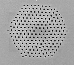
Optical fibers are fundamental to the information age and are now used not only for long-distance telecommunications but also for chemical sensing, fiber lasers, laser power delivery, and imaging, among many other applications. The fibers are drawn from silica or other types of glass or amorphous-polymer preforms. Because molten crystalline materials do not have viscosities compatible with fiber drawing, the useful material properties of optical fibers have been limited primarily to those of glass and polymer. If the material properties of crystalline semiconductors and metals could be integrated into optical fibers, many more fiber devices that generate, modulate, detect, or even guide or focus light at the nanoscale could become possible. We have developed a novel microfluidic chemical-deposition technique for fabrication of metal and semiconductor structures at dimensions down to the nanoscale within the pores of microstructured optical fibers (MOFs; see Fig. 1).
Chemical deposition onto the walls of the long, extremely narrow pores in MOFs does not seem feasible at first glance: the smallest deviation from perfect conformal deposition anywhere along the length of the pore would arrest deposition, and mass transport of the reactants into and byproducts out of such a confined space is prohibitively slow using traditional techniques. However, we found that high-pressure flow (2 to greater than 100 MPa), which can be sustained because of the high mechanical strength of the optical fibers, overcomes mass-transport constraints and enables a strikingly uniform, dense, and conformal annular deposition onto the heated pore walls. It was found that the hole from which deposition occurs could close down to less than 10 nm in diameter, allowing for fabrication of essentially solid wire waveguides and demonstrating the high perfection of the deposition process (see www.laserfocusworld.com/articles/255490).1 The process is strikingly simple, involving heating only very small quantities of a high-pressure precursor constrained within the interior of the MOFs (see Fig. 2).Microstructured optical fibers fabricated at the Southampton Optoelectronics Research Centre (ORC) can have dense arrays of capillaries with diameters down to nanoscale dimensions (10 to 100 nm) and lengths from meters to kilometers. The fibers can be engineered to have virtually any desired periodic or aperiodic spatial configuration. Silica MOFs are thus versatile nanotemplates that have extreme aspect ratio, are highly scalable, possess engineered geometries combined with unparalleled optical transparency, and tensile strength ten times greater than that of steel. Thus, wire materials can be deposited within the templates in virtually any desired two-dimensional (2‑D) spatial configuration.
The added structural complexity of MOFs compared to conventional optical fibers means they exhibit completely new properties such as endlessly single-mode guidance, photonic bandgaps, and dispersion engineering for creating enhanced nonlinear effects such as supercontinuum generation. Microstructured optical fibers are a subset of a larger class of metamaterials that have been of great interest for novel applications ranging from negative-index materials to superlenses to chemical sensing. Incorporating precisely structured metals and semiconductor materials into MOFs thus greatly increases the possibilities for manipulating light within this platform.
Nanoscale guiding and imaging
Metal-filled fiber structures have already started to inspire a new body of research in “fiberized” plasmonic devices for applications in nonlinear optics and molecular sensing. Traditional plasmonic devices based on a 2-D geometry typically use a prism to phase-match the incoming radiation with the surface plasmon wave, adding unwanted bulk and complexity. In the unique guiding geometry of MOFs, the silica core acts as a prism to couple transmitted light with plasmons at the air-metal interface.
Based on this approach, researchers have conducted several theoretical studies of the transmission properties of metal-dielectric MOF devices ranging from fibers with thin coatings on the capillary walls to solid nanowire inclusions. The results have shown that careful choice of the metal thickness and the design of the MOF can determine the wavelength, the number of plasmon resonances, and the losses within the device (see “Tuning of surface plasmons leads to new optoelectronic devices,” p. 103). A key advantage of our high-pressure chemical fluid-deposition technique is the ability to organize potentially thousands to millions of nanowires of metal, semiconductors, and dielectrics in highly ordered arrays within the cross section of a fiber. This enables a new class of nanoscale imaging ideas that will affect a broad range of science and technology fields, such as materials science, biological imaging, nanolithography, and endoscopy.
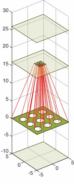
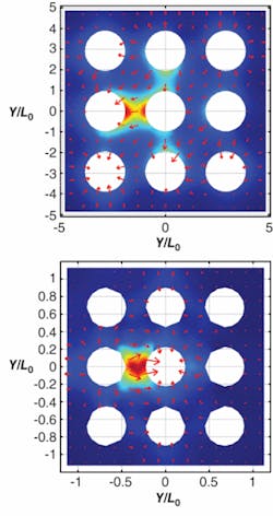
As an illustrative example, an endoscopic “nanocamera” could instantaneously capture an image with thousands of pixels with a resolution well below the diffraction limit (much less than λ/2 and possibly as small as λ/10 to λ/25). Near-field scanning optical microscopy is an established scanning-probe technique that uses a nanoscale aperture and tapered fibers to achieve approximately 40 nm resolution in the visible region of the spectrum. A nanocamera, in comparison, would not require serial scanning, thus allowing for very rapid imaging of structures that are difficult to image serially, such as living cells.Other proposed concepts to image at resolutions beyond the diffraction limit include superlenses, coupled-sphere waveguides, and resonantly excited surface-plasmon polaritons in arrays of metal wires.2 Shvets, Trendafilov, Pendry, and Sarychev propose an endoscopic nanocamera design consisting of an array of metallic nanowires embedded in a tapered optical fiber that can magnify and demagnify an image (see Fig. 3).3 They explain that if the taper cross section becomes smaller than λ2/4, then all the transverse electric (TE) and transverse magnetic (TM) modes of the light become evanescent. Therefore, the only propagating modes are TEM modes that are transverse local-in other words, an image of finite lateral size does not disperse as it propagates along a uniform cylindrical fiber. In a tapered fiber, however, the taper determines the magnification and demagnification (see Fig. 4). Moreover, the number of pixels in each camera can number in the thousands per fiber for a real imaging application.
For perfectly electrically conducting metal wires, the TEM modes are dispersionless with respect to any transverse wavevector, and hence are transverse local. In reality, this assumption is true only for far-infrared and terahertz wavelengths where real metals have very low loss, and hence this tapered-fiber imaging scheme will work well for these frequency ranges. However, in the mid-to near-infrared and visible frequency ranges, effects due to the excitation of surface-plasmon polaritons (SPPs) become an important consideration. Varying the metal wire height, diameter, and relative spacings effectively tunes the SPP resonances at different wavelengths. For example, subwavelength imaging with a resolution of 40 nm using a metallic silver nanowire array (20 nm diameter, 50 nm long, and spaced 40 nm apart in a hexagonal geometry) has been numerically modeled by Ono , Kato, and Kawata at 488 nm wavelength.2 The Shvets proposal does not depend on an SPP resonance. However, scaling to near-infrared wavelengths requires metal-wire radii that begin to approach the skin depth, which will result in crosstalk between wires. Thus, the Shvets concept is ideally suited for mid-infrared and longer wavelengths.
Finally, the taper itself provides a key advantage to the nanocamera idea, namely, that it magnifies the pixels in the image so that conventional silicon and germanium readout chips can detect them. If a typical photodetector pixel size is 5 µm, and an imaging resolution of 50 nm is desired, a magnification of 100× is needed. Calculations by Shvets et al., show that a maximum taper slope of 45° is allowed before the crosstalk between wires causes image spreading. For gentler tapers, this is not an issue with the TEM-mode imaging.
As yet, no obvious conventional method exists for fabricating a nanocamera such as Shvets and his colleagues describe. However, the high-pressure fiber-filling process is well suited for fabricating arrays of metal nanowires. Existing taper fabrication methods work on both conventional and microstructured optical fibers. Once the taper is constructed, the high-pressure filling process will facilitate ordered arrays of nanowires with a large range of different metals via suitable chemical-vapor deposition processes. Characterization of the light-guiding and imaging properties would then follow. The resulting endoscopic nanocamera would be useful for rapid nanoscale imaging over micron-square areas and would thus find application in areas ranging from biology and medicine to advanced materials research.
REFERENCES
1. P. J. Sazio et al., Science311, 1583 (2006).
2. A. Ono et al., Phys. Rev. Lett.95, 267407 (2005).
3. G. Shvets et al., Phys. Rev. Lett.99, 053903 (2007).
VENKATRAMAN GOPALAN is associate professor of materials science and engineering and JOHN V. BADDING is associate professor of chemistry at Pennsylvania State University, University Park, PA 16802; e-mail: [email protected]; tanzanite.chem.psu.edu. Pier Sazio is senior research fellow and Anna Peacock is senior research fellow at the Optoelectronics Research Centre, University of Southampton, Southampton, SO17 1BJ, England.


