NANOPHOTONICS: Direct-write nanopatterning uses optically trapped microspheres
In an extension of nanopatterning methods that use self-assembled microspheres, researchers at Princeton University (Princeton, NJ) are able to perform subwavelength direct-write nanopatterning using an optically trapped microsphere.1 The microsphere essentially acts as a near-field lens that can pattern surfaces with subwavelength features, without the need for sophisticated feedback systems to monitor probe/substrate spacings, as required by other multiphoton-absorption or near-field scanning optical-microscope techniques.
Polystyrene or silica microspheres with diameters of hundreds of nanometers are suspended in fluid between a glass coverslip and the coated substrate to be patterned (typically polyimide). A 532 nm green laser traps a particle in a Bessel-beam optical trap, while a 355 nm pulsed laser illuminates the microsphere and is focused onto the translating substrate to produce features on the order of 100 nm—three times smaller than the wavelength of light used for nanopatterning.
Unlike conventional optical tweezers, Bessel-beam traps confine particles in two dimensions with a scattering force in the propagation direction. Electrostatic repulsions between the charged surfaces of the microsphere and the substrate balance this scattering force, creating an equilibrium spacing on the order of 50 nm, depending on the laser characteristics and substrate/chemical characteristics of the Bessel-beam trap. As a result, the sphere can be self-positioned in the propagation direction with an accuracy of 10 nm, eliminating the need for feedback control between the sphere and its position above the substrate.
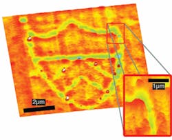
Both experimental and finite-difference time-domain simulations show that for 0.76-µm-diameter microspheres (an optimal diameter to produce small feature sizes while maintaining good positioning accuracy within the optical trap, unlike smaller microspheres), 130-nm-wide spot sizes at low laser fluences are produced on average, with a standard deviation of 38 nm. Higher laser energy (more than 40 mJ/cm2) causes increased feature size and raises the patterned surface, leaving a crater in the center. With the use of a pulsed laser and careful overlapping of the laser spots as the substrate is translated, a variety of continuous features can be fabricated (see figure). For an experimental continuous-line trench with a 38 nm standard deviation of the central minimum and a mean full width at half maximum of 263 nm, a positional accuracy of 30 nm can be achieved.
“One of the most important aspects of this work is the use of Bessel traps to self-position the microbeads above the surface,” says Craig B. Arnold, assistant professor of mechanical and aerospace engineering. “Self-positioning of the probe not only enables the creation of nanopatterns over nonplanar surfaces, but it also allows one to easily scale up the process by producing parallel arrays of Bessel traps, each of which can independently control the position of a microbead. This type of parallization gives rise to high-throughput direct-write nanopatterning that cannot easily be accomplished with other methods. In the future, we can envision this approach extending into a complete nanopatterning toolkit. For instance, by placing microparticles with different shapes and sizes in the same solution, researchers merely have to select the appropriate particle with their optical trap and directly create the desired features.”
REFERENCE
1. E. McLeod and C.B. Arnold, Nature Nanotechnology online, http://www.nature.com/nnano/journal/vaop/ncurrent/
abs/nnano.2008.150.html (June 8, 2008).

Gail Overton | Senior Editor (2004-2020)
Gail has more than 30 years of engineering, marketing, product management, and editorial experience in the photonics and optical communications industry. Before joining the staff at Laser Focus World in 2004, she held many product management and product marketing roles in the fiber-optics industry, most notably at Hughes (El Segundo, CA), GTE Labs (Waltham, MA), Corning (Corning, NY), Photon Kinetics (Beaverton, OR), and Newport Corporation (Irvine, CA). During her marketing career, Gail published articles in WDM Solutions and Sensors magazine and traveled internationally to conduct product and sales training. Gail received her BS degree in physics, with an emphasis in optics, from San Diego State University in San Diego, CA in May 1986.
