Silicon Photonics: Low-cost on-chip optical spectrometers have high channel count and signal-to-noise ratio
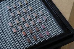
Researchers at the Massachusetts Institute of Technology (MIT; Cambridge, MA) are developing miniature chip-based spectrometers that are just as accurate and powerful as conventional large devices with six-figure price tags. The new spectrometers could be mass-produced using standard chipmaking processes (see figure).1 This approach could open up new uses for spectrometry that previously would have been physically and financially impossible.
Called the digital Fourier-transform (dFT) spectrometer, the device contains a reconfigurable Mach-Zehnder interferometer (MZI)] with optical switches on each arm that direct light to waveguides of different and unique path lengths, scaled in powers of two. As a result, the channel count scales exponentially with the number of optical switches. This is in contrast to other chip-based approaches that add one device per channel, resulting in a linear scaling.
Other groups have tried to make chip-based spectrometers, but there is a built-in challenge: A device’s ability to spectrally disperse light using any conventional optical system is highly dependent on the device’s size. “If you make it smaller, the performance degrades,” says JueJun Hu, one of the researchers.
Another type of spectrometer uses the Fourier-transform approach. However, these devices are still limited by the same size constraint—long optical paths are essential to attaining high performance.
Robust due to chip-based configuration
In the new MIT system, electro-optical switches eliminate the need for movable mirrors and can easily be fabricated using standard chipmaking technology. By eliminating the moving parts, says Derek Kita, another of the researchers, “there’s a huge benefit in terms of robustness. You could drop it off the table without causing any damage.”
As a proof of concept, the researchers contracted an industry-standard semiconductor manufacturing service to build a device operating at the telecommunication C-band between 1550 and 1570 nm with six sequential switches, producing 64 spectral channels, with built-in processing capability to control the device and process its output. By expanding to 10 switches, the resolution would jump to 1024 channels. They designed the device as a plug-and-play unit that could be easily integrated with existing optical networks.
The team also used new machine-learning techniques to reconstruct detailed spectra from a limited number of channels. The techniques resulted in significant noise suppression spectral-resolution enhancement beyond the classical Rayleigh criterion: the minimum resolvable wavelength detuning between two laser lines measured by the device was 0.2 nm, significantly better than the Rayleigh criterion of 0.4 nm.
The machine-learning method they developed works well to detect both broad and narrow spectral peaks, Kita says. They were able to demonstrate that its performance did indeed match the calculations, and thus opens up a wide range of potential further development for various applications.
The researchers say such spectrometers could find applications in sensing devices, materials analysis systems, optical coherence tomography in medical imaging, and monitoring the performance of optical networks, upon which most digital networks rely. Already, the team has been contacted by some companies interested in possible uses for such microchip spectrometers, with their promise of huge advantages in size, weight, and power consumption, Kita says. There is also interest in applications for real-time monitoring of industrial processes, Hu adds, as well as for environmental sensing for industries such as oil and gas.
REFERENCE
1. D. M. Kita et al., Nat. Commun. (2018); https://doi.org/10.1038/s41467-018-06773-2.

John Wallace | Senior Technical Editor (1998-2022)
John Wallace was with Laser Focus World for nearly 25 years, retiring in late June 2022. He obtained a bachelor's degree in mechanical engineering and physics at Rutgers University and a master's in optical engineering at the University of Rochester. Before becoming an editor, John worked as an engineer at RCA, Exxon, Eastman Kodak, and GCA Corporation.
