Solar-blind UV photodetector has nanocrystals synthesized by using ion implantation
Scientists at Lobachevsky University (UNN; Nizhnij Novgorod, Russia), the Indian Institute of Technology Jodhpur, and the Indian Institute of Technology Ropar have been working to develop solar-blind photodetectors operating in the ultraviolet (UV) spectral band. In the field of electronic technology, this is an important task since such devices cut off emission with a wavelength higher than 280 nm, which helps to avoid interference from sunlight and to record UV emission during daylight. Solar-blind photodetectors provide a wide range of important applications, including ozone-damage detection, jet-engine monitoring, and flame detection. The main materials for creating solar-blind photodetectors are wide-gap semiconductors. The researchers consider gallium oxide (Ga2O3) to be a promising semiconductor with a bandgap of 4.4 to 4.9 eV, which cuts off emission with wavelengths higher than 260 to 280 nm and is capable of detecting emission in the deep-UV range.
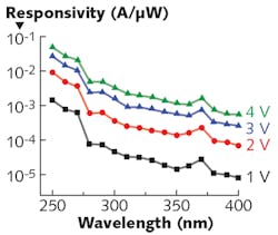
Existing methods for Ga2O3 synthesis are quite complicated and poorly compatible with conventional silicon technologies. In addition, the layers obtained by such methods often have many defects. The synthesis of Ga2O3 nanocrystals by means of ion implantation, the basic technology of modern electronics, opens up possibilities for creating solar-blind photodetectors. The spectral photoresponse for this photodetector shows excellent solar-blind UV characteristics in the 250 to 270 nm range—the detector also has a high responsivity of 50 mA/μW at 250 nm. The 0.168 mA dark current of the photodetector is quite low.
The process of creating such a detector involves the synthesis of Ga2O3 nanocrystals in an aluminum oxide (Al2O3) film on silicon by ion implantation. A detector fabricated in this way has been realized by the UNN scientists for the first time. Reference: S. Rajamani et al., IEEE Sensors J. (2018); doi:10.1109/jsen.2018.2821562.

John Wallace | Senior Technical Editor (1998-2022)
John Wallace was with Laser Focus World for nearly 25 years, retiring in late June 2022. He obtained a bachelor's degree in mechanical engineering and physics at Rutgers University and a master's in optical engineering at the University of Rochester. Before becoming an editor, John worked as an engineer at RCA, Exxon, Eastman Kodak, and GCA Corporation.
