Quantum-dot-based Light Sources: Perovskite quantum-dot superlattices produce superfluorescent quantum light

Up to now, superfluorescence—the spontaneous, collective, coherent emission of radiation by an ensemble of quantum emitters confined in a small volume—has been possible in some gases and some semiconductor crystals. But thanks to fabrication advances that have improved the physical uniformity of cesium lead-halide perovskite quantum dots (QDs), researchers at ETH Zurich (Zurich, Switzerland), Empa (Dübendorf, Switzerland), and IBM Research – Zurich have successfully demonstrated superfluorescence from perovskite QD superlattices that boost optoelectronic device performance and could serve as the basis for entangled multiphoton quantum light sources.1
Superlattice fabrication and emission
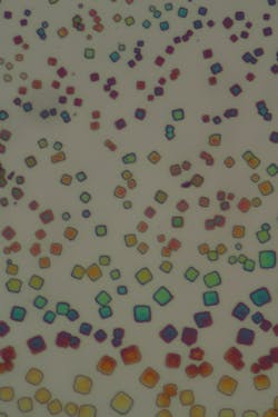
Superfluorescence depends on emission uniformity of the nanocrystals within the confined volume. In addition, the emitters have to exhibit high coupling strength to the light field and a long coherence time. Essentially, superlattices are three-dimensional (3D) structures composed of individual colloidal nanocrystals (see figure). After fabricating CsPbX3 (X = Cl, Br) nanocrystalline QDs with a mean size of 10 nm and size deviation of <5%, a series of chemical purifications and centrifuge processes followed by evaporation steps is used to create superlattices with a lateral size of up to 5 µm spread over a 5 × 7 mm area. Each superlattice contains several million well-ordered nanocrystals.
The photoluminescence spectrum of a single superlattice consists of two peaks: a high-energy emission peak that coincides with the peak produced by individual nanocrystals within a superlattice and is therefore attributed to uncoupled QD emission; and a narrow, red-shifted (by 70 to 90 meV) peak that is attributed to cooperative, coupled QD emission.
When the optical excitation fluence is increased, the photoluminescence decay time of the coupled QD emission is accelerated up to more than 20X compared to the uncoupled QD emission. Emission from coupled QDs leads to a multiphoton emission burst (and photon bunching), because the spontaneous coherent coupling enables the emission of highly correlated multiple photons within a time interval as short as 10 ps.
This is the result of the strong quantum-mechanical interactions among individual nanocrystals mediated by the common vacuum modes, which leads to the formation of a single, giant emitting dipole from all participating QDs.
“As superfluorescence can now be achieved in a technologically relevant material system with low-cost synthesis and easy processing, it could be explored to boost the performance of QD-based optoelectronic devices and opens up new opportunities for the development of high-brightness and multiphoton quantum light sources—a key missing resource for quantum sensing, quantum-encrypted communication, and future quantum computing,” says Gabriele Rainò, senior researcher at ETH-Zurich.
REFERENCE
1. G. Rainò et al., Nat. Lett. (Nov. 7, 2018); https://www.nature.com/articles/s41586-018-0683-0.
About the Author

Gail Overton
Senior Editor (2004-2020)
Gail has more than 30 years of engineering, marketing, product management, and editorial experience in the photonics and optical communications industry. Before joining the staff at Laser Focus World in 2004, she held many product management and product marketing roles in the fiber-optics industry, most notably at Hughes (El Segundo, CA), GTE Labs (Waltham, MA), Corning (Corning, NY), Photon Kinetics (Beaverton, OR), and Newport Corporation (Irvine, CA). During her marketing career, Gail published articles in WDM Solutions and Sensors magazine and traveled internationally to conduct product and sales training. Gail received her BS degree in physics, with an emphasis in optics, from San Diego State University in San Diego, CA in May 1986.