Advances in Detectors: The Quanta image sensor (QIS): Making every photon count
ERIC R. FOSSUM and KAITLIN ANAGNOST
A new paradigm for image sensing and capture was suggested in 2005 that led to what is now called the Quanta image sensor (QIS).1 In the QIS, photoelectrons are counted one by one, and an image is computed from combined spatial and temporal photon-count data.
A room-temperature photon-counting image sensor implemented in a slightly modified mainstream CMOS image sensor (CIS) 3D stacked, backside illumination (BSI) fabrication process that does not use avalanche multiplication, the QIS consists of specialized, low-full-well-capacity, sub-diffraction-limit pixels called jots. Their full-well capacity is just a few electrons and deep sub-electron read noise (DSERN)—less than 0.3 e- root-mean squared (RMS)—is attained without the use of avalanche multiplication. DSERN allows binary output of the QIS, reflecting the absence or presence of a photoelectron.
The QIS may contain hundreds of millions or possibly billions of jots with readout speed of perhaps 1000 frames per second (fps) or higher, leading to raw data rates approaching 1 Tbit/s. Application-specific data reduction can be contemplated in stacked architecture of the QIS and using advanced denoising algorithms, good grayscale images can be captured in extreme low light of less than one photon per pixel on average.
Photon-counting image sensors, like the QIS, represent a different way to create images compared to CMOS image sensors and their ancestor, the charge-coupled device (CCD). In those devices, the signal photocharge is integrated in analog in the sensor and digitized to 8–14 bits of resolution at readout. The full-well capacity defines the upper end of the dynamic range, and the read noise, often in the 1–3 e- RMS range, defines the lower end. For monochrome sensors, an output image pixel is the digitized value of the charge collected in one sensor pixel.
On the other hand, in a photon-counting image sensor such as the QIS, the signal is digitally integrated on- or off-chip and an image pixel is computationally formed from a spatiotemporal cubicle of jot values (see Fig. 1). While it images one photon at a time (or sometimes more in a multibit QIS), high dynamic range (>120 dB) can still be achieved using the intrinsic overexposure latitude of the QIS and multiple high-speed exposure techniques.2 Photon-counting image sensors, however, do not perform well in one area: flash photography, wherein many photons arrive at the pixel simultaneously.
Sensing single photoelectrons
Sensing a single photoelectron is difficult because the electron charge, 1.6 × 10⁻¹⁹ C, is very small and the resultant voltage is typically less than the noise level of the readout circuit. Input-referred readout noise in CMOS image sensors, including scientific CMOS (sCMOS), are typically in the range of 1 to 5 e- RMS, but photon-counting typically requires DSERN levels. The solution is to provide gain without introducing additional noise.
The QIS being pursued at Dartmouth started with a baseline CIS process, with small modifications made to invent a new pixel device structure called the pump-gate jot.3 This structure has very low sense capacitance, yielding a conversion gain of hundreds of microvolts per electron—enough for overcoming other readout noise sources. Aside from this modification, features of the highly evolved CIS process are maintained, including BSI and 3D stacking.
All other photon-counting devices, such as single-photon avalanche diode (SPAD) and electron-multiplying CCD (EMCCD) detectors, use avalanche multiplication to achieve enough charge gain for photon sensing, but must contend with avalanche multiplication’s numerous downsides.
The avalanche process leads to variance in the charge gain. The high electric field required for operation of the device makes it very sensitive to silicon defects, leading to high dark count rates that limit performance and manufacturing yield. The devices are typically quite sensitive to biasing and clocking voltages, and the high electric fields also make pixel-shrink challenging because of crosstalk and isolation needs. Thus, devices using avalanche multiplication tend to have much larger pixels and lower resolution than the QIS—typically a few hundred thousand pixels for SPAD arrays and a megapixel for EMCCDs.
As a result of the way a SPAD works, SPADs are not well suited for photon-number resolution since a single photon propels the device into Geiger mode and it must be reset before the next count is possible, leading to detection dead time. Also, EMCCDs have additional noise sources that make photon-number resolution challenging. On the other hand, SPADs have shown unrivaled suitability for photon-arrival time resolution. With the addition of in-pixel timing circuits, SPADs have found mass application in time-of-flight (TOF) imaging.
Million-pixel photon-counting test device
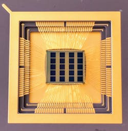
Dartmouth, in collaboration with the Taiwan Semiconductor Manufacturing Corporation (TSMC; Hsinchu, Taiwan), has implemented a test chip in a 45/65 nm 3D stacked BSI CIS process.4 Device design, layout, verification, and characterization were performed at Dartmouth.
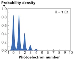
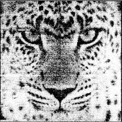
The test chip consisted of 20 different 1 Mjot QIS arrays, each with pixel pitch of 1.1 µm and shared readout. Half of the arrays were analog output and the other half were single-bit digital output—several different jot designs were characterized. A 3D-stacked cluster-parallel readout architecture was implemented that permits ready scaling of array size. The read noise, conversion gain, dark current, and other normal image sensor parameters were tested with the analog output using a high-resolution analog-to-digital converter (ADC) operated at relatively slow output speeds. The binary output arrays were tested at 1000 fps or 1 Gpix/s (see Fig. 2).The photon counting histogram made from 20,000 reads shows clear quantization in signals corresponding to different numbers of electrons. The relative peak heights follow Poisson statistics and the average photoelectron number (quanta exposure) can be characterized by the pattern, yielding 1.01 e-. The separation between peaks provides a second and, in fact, more accurate method of determining conversion gain.
QIS and SPADs
The QIS can be realized by different types of photon-counting pixels. In the Dartmouth device, a CIS baseline process was used that does not use avalanche multiplication, leading to smaller pixel sizes, low power dissipation, low dark count rates, and likely improved manufacturing yield. It is easy to envision such a device being scaled to 10, 100, or 1000 million pixels, depending on the application.
These CIS-based QIS devices can be extended to a multibit mode where instead of single-bit quantization, low bit-depth quantization (such as 3b) is used to improve flux capacity without significantly impacting high-speed readout or power dissipation.
With time-resolved applications like TOF imaging that have entered mass production, SPAD arrays have been around for more than a decade and have matured considerably. Since the introduction of the QIS concept, SPADs have been used to successfully demonstrate much of the predicted QIS performance and operation.5
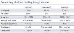
It is possible, with 3D stacking technology and continued SPAD pixel shrinkage, that the performance of SPADs will make them viable for low-resolution (1-10 Mpixel) QIS applications in the future. However, the intrinsic advantage of using a CIS process will lead to unmatched pixel and resolution scaling with reduced die size, cost, and power, with higher manufacturing yield and lower cost per die (see table).QIS applications
Photon-counting image sensors such as the QIS, SPAD arrays, and EMCCDs provide glimpses of our world—one photon at a time. In ultralow-light applications, such as for scientific imaging in the life sciences or astronomy, or in low-light aerospace and defense and security applications, photon-counting imaging is critical.
Low-power QIS devices will also find application in low-light Internet of Things (IoT) applications, especially if computational image formation is done in the cloud. Other potential applications, including quantum cryptography and cinematography, are being explored by the Dartmouth spinoff startup Gigajot Technology (Pasadena, CA). Due to the myriad of possibilities offered by computational imaging, it is possible that a QIS device might ultimately find its way to your smartphone.
ACKNOWLEDGMENTS
Eric R. Fossum is grateful for the pioneering work done by his former and current PhD students, especially Jiaju Ma and Saleh Masoodian both currently at Gigajot, and Dakota Starkey and Wei Deng. The support of Rambus (Sunnyvale, CA) and TSMC is gratefully acknowledged.
REFERENCES
1. E. R. Fossum, “What to do with sub-diffraction limit (SDL) pixels? – a proposal for a gigapixel digital film sensor (DFS),” IEEE Workshop on CCDs and Adv. Image Sensors, Karuizawa, Japan (Jun. 2005).
2. E. R. Fossum et al., Sensors, 16, 8, 1260 (Aug. 2016).
3. J. Ma and E. R. Fossum, IEEE J. Electron Devices, 3, 2, 73–77 (Mar. 2015).
4. J. Ma et al., Optica, 4, 12, 1474–1481 (December 2017).
5. N. A. W. Dutton et al., Sensors, 16, 7, 1122 (2016).
6. See https://goo.gl/JkxWgG.
Eric R. Fossum is the John H. Krehbiel Sr. Professor for Emerging Technologies and Kaitlin Anagnost is a first-year PhD engineering student, both at the Thayer School of Engineering at Dartmouth College, Hanover, NH; e-mail: [email protected]; www.dartmouth.edu.

